SLVS503F November   2003  – February 2020 TPS2490 , TPS2491

PRODUCTION DATA.  

  1. Features
  2. Applications
  3. Description
    1.     Device Images
      1.      Typical Application
  4. Revision History
  5. Pin Configuration and Functions
    1.     Pin Functions
  6. Specifications
    1. 6.1 Absolute Maximum Ratings
    2. 6.2 ESD Ratings
    3. 6.3 Recommended Operating Conditions
    4. 6.4 Thermal Information
    5. 6.5 Electrical Characteristics
    6. 6.6 Switching Characteristics
    7. 6.7 Typical Characteristics
  7. Detailed Description
    1. 7.1 Overview
    2. 7.2 Functional Block Diagram
    3. 7.3 Feature Description
      1. 7.3.1  VCC
      2. 7.3.2  SENSE
      3. 7.3.3  GATE
      4. 7.3.4  OUT
      5. 7.3.5  EN
      6. 7.3.6  VREF
      7. 7.3.7  PROG
      8. 7.3.8  TIMER
      9. 7.3.9  PG
      10. 7.3.10 GND
    4. 7.4 Device Functional Modes
      1. 7.4.1 Board Plug-In ()
      2. 7.4.2 TIMER and PG Operation ()
      3. 7.4.3 Action of the Constant Power Engine ()
      4. 7.4.4 Response to a Hard Output Short ( and )
      5. 7.4.5 Automatic Restart ()
  8. Application and Implementation
    1. 8.1 Application Information
      1. 8.1.1 Alternative Inrush Designs
        1. 8.1.1.1 Gate Capacitor (dV/dt) Control
        2. 8.1.1.2 PROG Inrush Control
      2. 8.1.2 Additional Design Considerations
        1. 8.1.2.1 Use of PG
        2. 8.1.2.2 Faults and Backplane Voltage Droop
        3. 8.1.2.3 Output Clamp Diode
        4. 8.1.2.4 Gate Clamp Diode
        5. 8.1.2.5 High Gate Capacitance Applications
        6. 8.1.2.6 Input Bypass
        7. 8.1.2.7 Output Short Circuit Measurements
    2. 8.2 Typical Application
      1. 8.2.1 Design Requirements
      2. 8.2.2 Detailed Design Procedure
        1. 8.2.2.1 Select RSNS and CL setting
        2. 8.2.2.2 Selecting the Hot Swap FET(s)
        3. 8.2.2.3 Select Power Limit
        4. 8.2.2.4 Set Fault Timer
        5. 8.2.2.5 Check MOSFET SOA
        6. 8.2.2.6 Set Under-Voltage Threshold
        7. 8.2.2.7 Choose R5, and CIN
        8. 8.2.2.8 Input and Output Protection
        9. 8.2.2.9 Final Schematic and Component Values
      3. 8.2.3 Application Curves
  9. Power Supply Recommendations
  10. 10Layout
    1. 10.1 Layout Guidelines
      1. 10.1.1 PC Board Guidelines
      2. 10.1.2 System Considerations
    2. 10.2 Layout Example
  11. 11Device and Documentation Support
    1. 11.1 Development Support
    2. 11.2 Documentation Support
      1. 11.2.1 Related Documentation
    3. 11.3 Related Links
    4. 11.4 Receiving Notification of Documentation Updates
    5. 11.5 Community Resources
    6. 11.6 Trademarks
    7. 11.7 Electrostatic Discharge Caution
    8. 11.8 Glossary
  12. 12Mechanical, Packaging, and Orderable Information

封装选项

请参考 PDF 数据表获取器件具体的封装图。

机械数据 (封装 | 引脚)
  • DGS|10
散热焊盘机械数据 (封装 | 引脚)
订购信息

Application Curves

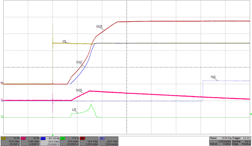
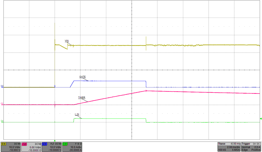
TPS2490 TPS2491 tps2490_startup.gif
Figure 20. Start-Up
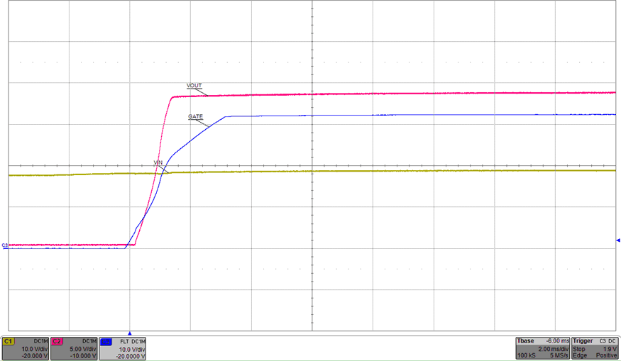
TPS2490 TPS2491 tps2490_undervoltage.gif
Figure 22. Under-Voltage
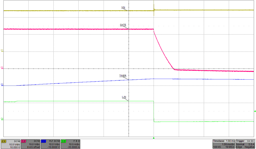
TPS2490 TPS2491 tps2490_load_step.gif
Figure 24. Loadstep
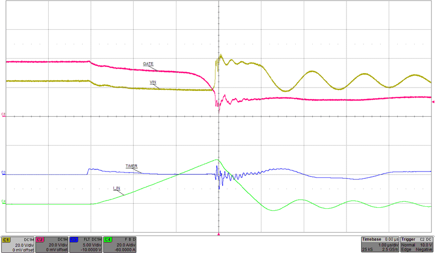
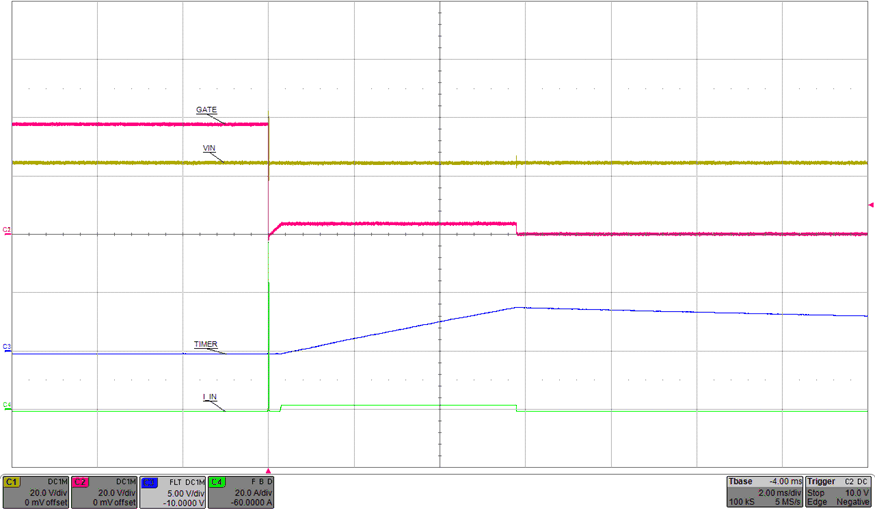
TPS2490 TPS2491 tps2490_hot_short_zoomed.gif
Figure 26. Hotshort (Zoomed-In)
TPS2490 TPS2491 tps2490_start_into_short.gif
Figure 21. Start-Up into Short Circuit
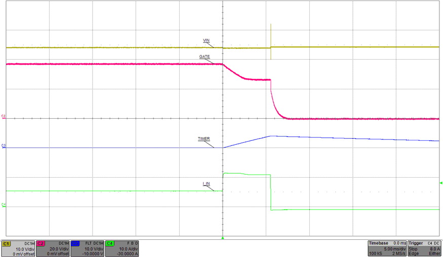
TPS2490 TPS2491 tps2490_gradual_overcurrent.gif
Figure 23. Gradual Over-Current
TPS2490 TPS2491 tps2490_hot_short.gif
Figure 25. Hotshort on Output