SLVS503F November   2003  – February 2020 TPS2490 , TPS2491

PRODUCTION DATA.  

  1. Features
  2. Applications
  3. Description
    1.     Device Images
      1.      Typical Application
  4. Revision History
  5. Pin Configuration and Functions
    1.     Pin Functions
  6. Specifications
    1. 6.1 Absolute Maximum Ratings
    2. 6.2 ESD Ratings
    3. 6.3 Recommended Operating Conditions
    4. 6.4 Thermal Information
    5. 6.5 Electrical Characteristics
    6. 6.6 Switching Characteristics
    7. 6.7 Typical Characteristics
  7. Detailed Description
    1. 7.1 Overview
    2. 7.2 Functional Block Diagram
    3. 7.3 Feature Description
      1. 7.3.1  VCC
      2. 7.3.2  SENSE
      3. 7.3.3  GATE
      4. 7.3.4  OUT
      5. 7.3.5  EN
      6. 7.3.6  VREF
      7. 7.3.7  PROG
      8. 7.3.8  TIMER
      9. 7.3.9  PG
      10. 7.3.10 GND
    4. 7.4 Device Functional Modes
      1. 7.4.1 Board Plug-In ()
      2. 7.4.2 TIMER and PG Operation ()
      3. 7.4.3 Action of the Constant Power Engine ()
      4. 7.4.4 Response to a Hard Output Short ( and )
      5. 7.4.5 Automatic Restart ()
  8. Application and Implementation
    1. 8.1 Application Information
      1. 8.1.1 Alternative Inrush Designs
        1. 8.1.1.1 Gate Capacitor (dV/dt) Control
        2. 8.1.1.2 PROG Inrush Control
      2. 8.1.2 Additional Design Considerations
        1. 8.1.2.1 Use of PG
        2. 8.1.2.2 Faults and Backplane Voltage Droop
        3. 8.1.2.3 Output Clamp Diode
        4. 8.1.2.4 Gate Clamp Diode
        5. 8.1.2.5 High Gate Capacitance Applications
        6. 8.1.2.6 Input Bypass
        7. 8.1.2.7 Output Short Circuit Measurements
    2. 8.2 Typical Application
      1. 8.2.1 Design Requirements
      2. 8.2.2 Detailed Design Procedure
        1. 8.2.2.1 Select RSNS and CL setting
        2. 8.2.2.2 Selecting the Hot Swap FET(s)
        3. 8.2.2.3 Select Power Limit
        4. 8.2.2.4 Set Fault Timer
        5. 8.2.2.5 Check MOSFET SOA
        6. 8.2.2.6 Set Under-Voltage Threshold
        7. 8.2.2.7 Choose R5, and CIN
        8. 8.2.2.8 Input and Output Protection
        9. 8.2.2.9 Final Schematic and Component Values
      3. 8.2.3 Application Curves
  9. Power Supply Recommendations
  10. 10Layout
    1. 10.1 Layout Guidelines
      1. 10.1.1 PC Board Guidelines
      2. 10.1.2 System Considerations
    2. 10.2 Layout Example
  11. 11Device and Documentation Support
    1. 11.1 Development Support
    2. 11.2 Documentation Support
      1. 11.2.1 Related Documentation
    3. 11.3 Related Links
    4. 11.4 Receiving Notification of Documentation Updates
    5. 11.5 Community Resources
    6. 11.6 Trademarks
    7. 11.7 Electrostatic Discharge Caution
    8. 11.8 Glossary
  12. 12Mechanical, Packaging, and Orderable Information

封装选项

请参考 PDF 数据表获取器件具体的封装图。

机械数据 (封装 | 引脚)
  • DGS|10
散热焊盘机械数据 (封装 | 引脚)
订购信息

Response to a Hard Output Short (Figure 15 and Figure 16)

Figure 15 shows the short circuit response over the full time-out period. The period begins when the output voltage falls and ends when Q1 is turned off. Q1 current is actively controlled by the constant power engine and gate amplifier circuit while the TIMER pin charges CT to the 4-V threshold causing Q1 to be turned off. The TPS2490 latches off after the threshold is reached until either the input voltage drops below the UVLO threshold or EN cycles through the false (low) state. The TPS2491 goes through a timing sequence before attempting a restart.
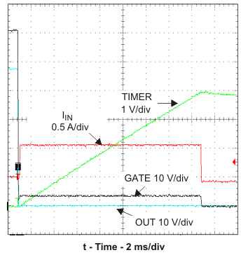
TPS2490 TPS2491 Ilim_Oview_lvs503.gifFigure 15. Current Limit Overview

The TPS249x responds rapidly to the short circuit as seen in Figure 16. The falling OUT voltage is the result of Q1 and CO currents through the short’s impedance at this time scale. The internal GATE clamp causes the GATE voltage to follow the output voltage down and subsequently limits the negative VGS to 1 V to 2 V. The rapidly rising fault current overdrives the GATE amplifier causing it to overshoot and rapidly turn Q1 off by sinking current to ground. Q1 slowly turns back on as the GATE amplifier recovers; Q1 then settles to an equilibrium operating point determined by the power limiting circuit.
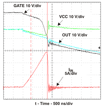
TPS2490 TPS2491 Ilim_Onset_lvs503.gifFigure 16. Current Limit Onset

Minimal input voltage overshoot appears in Figure 16 because a local 100-µF bypass capacitor and very short input leads were used. The input voltage would overshoot as the input current abruptly drops in a typical application due to the stored energy in the input distribution’s inductance. The exact waveforms seen in an application depend upon many factors including parasitics of the voltage distribution, circuit layout, and the short itself.