SLVS503F November   2003  – February 2020 TPS2490 , TPS2491

PRODUCTION DATA.  

  1. Features
  2. Applications
  3. Description
    1.     Device Images
      1.      Typical Application
  4. Revision History
  5. Pin Configuration and Functions
    1.     Pin Functions
  6. Specifications
    1. 6.1 Absolute Maximum Ratings
    2. 6.2 ESD Ratings
    3. 6.3 Recommended Operating Conditions
    4. 6.4 Thermal Information
    5. 6.5 Electrical Characteristics
    6. 6.6 Switching Characteristics
    7. 6.7 Typical Characteristics
  7. Detailed Description
    1. 7.1 Overview
    2. 7.2 Functional Block Diagram
    3. 7.3 Feature Description
      1. 7.3.1  VCC
      2. 7.3.2  SENSE
      3. 7.3.3  GATE
      4. 7.3.4  OUT
      5. 7.3.5  EN
      6. 7.3.6  VREF
      7. 7.3.7  PROG
      8. 7.3.8  TIMER
      9. 7.3.9  PG
      10. 7.3.10 GND
    4. 7.4 Device Functional Modes
      1. 7.4.1 Board Plug-In ()
      2. 7.4.2 TIMER and PG Operation ()
      3. 7.4.3 Action of the Constant Power Engine ()
      4. 7.4.4 Response to a Hard Output Short ( and )
      5. 7.4.5 Automatic Restart ()
  8. Application and Implementation
    1. 8.1 Application Information
      1. 8.1.1 Alternative Inrush Designs
        1. 8.1.1.1 Gate Capacitor (dV/dt) Control
        2. 8.1.1.2 PROG Inrush Control
      2. 8.1.2 Additional Design Considerations
        1. 8.1.2.1 Use of PG
        2. 8.1.2.2 Faults and Backplane Voltage Droop
        3. 8.1.2.3 Output Clamp Diode
        4. 8.1.2.4 Gate Clamp Diode
        5. 8.1.2.5 High Gate Capacitance Applications
        6. 8.1.2.6 Input Bypass
        7. 8.1.2.7 Output Short Circuit Measurements
    2. 8.2 Typical Application
      1. 8.2.1 Design Requirements
      2. 8.2.2 Detailed Design Procedure
        1. 8.2.2.1 Select RSNS and CL setting
        2. 8.2.2.2 Selecting the Hot Swap FET(s)
        3. 8.2.2.3 Select Power Limit
        4. 8.2.2.4 Set Fault Timer
        5. 8.2.2.5 Check MOSFET SOA
        6. 8.2.2.6 Set Under-Voltage Threshold
        7. 8.2.2.7 Choose R5, and CIN
        8. 8.2.2.8 Input and Output Protection
        9. 8.2.2.9 Final Schematic and Component Values
      3. 8.2.3 Application Curves
  9. Power Supply Recommendations
  10. 10Layout
    1. 10.1 Layout Guidelines
      1. 10.1.1 PC Board Guidelines
      2. 10.1.2 System Considerations
    2. 10.2 Layout Example
  11. 11Device and Documentation Support
    1. 11.1 Development Support
    2. 11.2 Documentation Support
      1. 11.2.1 Related Documentation
    3. 11.3 Related Links
    4. 11.4 Receiving Notification of Documentation Updates
    5. 11.5 Community Resources
    6. 11.6 Trademarks
    7. 11.7 Electrostatic Discharge Caution
    8. 11.8 Glossary
  12. 12Mechanical, Packaging, and Orderable Information

封装选项

请参考 PDF 数据表获取器件具体的封装图。

机械数据 (封装 | 引脚)
  • DGS|10
散热焊盘机械数据 (封装 | 引脚)
订购信息

System Considerations

A) Continued proper operation of the LM5069 hot swap circuit requires capacitance be present on the supply side of the connector into which the hot swap circuit is plugged in, as depicted in . The capacitor in the Live Backplane section is necessary to absorb the transient generated whenever the hot swap circuit shuts off the load current. If the capacitance is not present, inductance in the supply lines generate a voltage transient at shut-off which can exceed the absolute maximum rating of the TPS2490, resulting in its destruction.

B) If the load powered via the TPS2490 hot swap circuit has inductive characteristics, a diode is required across the TPS2490’s output. The diode provides a recirculating path for the load’s current when the TPS2490 shuts off that current. Adding the diode prevents possible damage to the TPS2490 as the OUT pin is taken below ground by the inductive load at shutoff. See Figure 27.
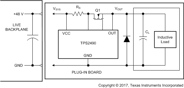
TPS2490 TPS2491 tps2490_output_schottky.gifFigure 27. Output Diode Required for Inductive Loads