ZHCS981A JUNE 2012 – August 2016 TPS2511
PRODUCTION DATA.
- 1 特性
- 2 应用范围
- 3 说明
- 4 修订历史记录
- 5 Pin Configuration and Functions
- 6 Specifications
-
7 Detailed Description
- 7.1 Overview
- 7.2 Functional Block Diagram
- 7.3
Feature Description
- 7.3.1 Overcurrent Protection
- 7.3.2 Current Limit Threshold
- 7.3.3 Current-Sensing Report (CS)
- 7.3.4 Undervoltage Lockout (UVLO) and Enable (EN)
- 7.3.5 Soft Start, Reverse Blocking, and Discharge Output
- 7.3.6 Thermal Sense
- 7.3.7 VBUS Voltage Drop Compensation
- 7.3.8 Divide Mode Selection of 5-W and 10-W USB Chargers
- 7.4 Device Functional Modes
- 8 Application and Implementation
- 9 Power Supply Recommendations
- 10Layout
- 11器件和文档支持
- 12机械、封装和可订购信息
7 Detailed Description
7.1 Overview
The following overview references various industry standards. TI always recommends consulting the latest standard to ensure the most recent and accurate information.
Rechargeable portable equipment requires an external power source to charge its batteries. USB ports are convenient locations for charging because of an available 5-V power source. Universally accepted standards are required to ensure host and client-side devices meet the power management requirements. Traditionally, USB host ports following the USB 2.0 Specification must provide at least 500 mA to downstream client-side devices. Because multiple USB devices can be attached to a single USB port through a bus-powered hub, it is the responsibility of the client-side device to negotiate the power allotment from the host to ensure the total current draw does not exceed 500 mA. The TPS2511 provides 100 mA of current to each USB device. Each USB device can subsequently request more current, which is granted in steps of 100 mA up 500 mA total. The host may grant or deny the request based on the available current.
Additionally, the success of the USB technology makes the micro-USB connector a popular choice for wall adapter cables. This allows a portable device to charge from both a wall adapter and USB port with only one connector.
One common difficulty has resulted from this. As USB charging has gained popularity, the 500-mA minimum defined by the USB 2.0 Specification or 900 mA defined in the USB 3.0 Specification, has become insufficient for many handsets, tablets, and personal media players (PMP), which have a higher-rated charging current. Wall adapters and car chargers can provide much more current than 500 mA or 900 mA to fast charge portable devices. Several new standards have been introduced defining protocol handshaking methods that allow host and client devices to acknowledge and draw additional current beyond the 500 mA (defined in the USB 2.0 Specification) or 900 mA (defined in the USB 3.0 Specification) minimum while using a single micro-USB input connector.
The TPS2511 supports three of the most common protocols:
- USB Battery Charging Specification, Revision 1.2 (BC1.2)
- Chinese Telecommunications Industry Standard YD/T 1591-2009
- Divider Mode
In these protocols there are three types of charging ports defined to provide different charging current to client-side devices. These charging ports are defined as:
- Standard downstream port (SDP)
- Charging downstream port (CDP)
- Dedicated charging port (DCP)
The BC1.2 Specification defines a charging port as a downstream facing USB port that provides power for charging portable equipment.
Table 1 lists different port operating modes according to the BC1.2 Specification.
Table 1. Operating Modes Table
| PORT TYPE | SUPPORTS USB 2.0 COMMUNICATION |
MAXIMUM ALLOWABLE CURRENT DRAWN BY PORTABLE EQUIPMENT (A) |
|---|---|---|
| SDP (USB 2.0) | Yes | 0.5 |
| SDP (USB 3.0) | Yes | 0.9 |
| CDP | Yes | 1.5 |
| DCP | No | 1.5 |
The BC1.2 Specification defines the protocol necessary to allow portable equipment to determine what type of port it is connected to so that it can allot its maximum allowable current drawn. The hand-shaking process is two steps. During step one, the primary detection, the portable equipment outputs a nominal 0.6-V output on its D+ line and reads the voltage input on its D– line. The portable device concludes it is connected to a SDP if the voltage is less than the nominal data detect voltage of 0.3 V. The portable device concludes that it is connected to a Charging Port if the D– voltage is greater than the nominal data detect voltage of 0.3 V and less than 0.8 V. The second step, the secondary detection, is necessary for portable equipment to determine between a CDP and a DCP. The portable device outputs a nominal 0.6-V output on its D– line and reads the voltage input on its D+ line. The portable device concludes it is connected to a CDP if the data line being remains is less than the nominal data detect voltage of 0.3 V. The portable device concludes it is connected to a DCP if the data line being read is greater than the nominal data detect voltage of 0.3 V and less than 0.8 V.
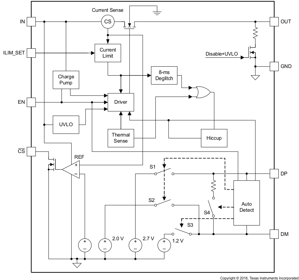
7.2 Functional Block Diagram
7.3 Feature Description
7.3.1 Overcurrent Protection
During an overload condition, the TPS2511 maintains a constant output current and reduces the output voltage accordingly. If the output voltage falls to less than 3.8 V for 16 ms, the TPS2511 turns off the output for a period of 12 seconds as shown in Figure 10. This operation is referred to as hiccup mode. The device stays in hiccup mode (power cycling) until the overload condition is removed. Therefore the average output current is significantly reduced to greatly improve the thermal stress of the device while the OUT pin is shorted.
 Figure 10. OUT Pin Short-Circuit Current in Hiccup Mode
Two possible overload conditions can occur. In the first condition, the output has been shorted before the device is enabled or before the voltage of IN has been applied. The TPS2511 senses the short and immediately switches into hiccup mode of constant-current limiting. In the second condition, a short or an overload occurs while the device is enabled. At the instant the overload occurs, high currents may flow for several microseconds before the current limit circuit can react. The device operates in constant-current mode for a period of 16 ms after the current limit circuit has responded, then switches into hiccup mode (power cycling).
7.3.2 Current Limit Threshold
The TPS2511 has a current limiting threshold that is externally programmed with a resistor. Equation 1 and Figure 11 help determine the typical current limit threshold.

where
- IOS_TYP is in mA and RILIM is in kΩ
- IOS_TYP has a better accuracy if RILIM is less than 210 kΩ
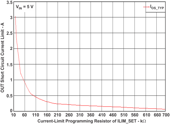 Figure 11. Typical Current Limit vs Programming Resistor
7.3.3 Current-Sensing Report (CS)
The CS open-drain output is asserted immediately when the OUT pin current is more than about half of the current limit set by a resistor on ILIM_SET pin. Built-in hysteresis improves the ability to resist current noise on the OUT pin. The CS output is active low. The recommended operating sink current is less than 2 mA and maximum sink current is 10 mA.
7.3.4 Undervoltage Lockout (UVLO) and Enable (EN)
The undervoltage lockout (UVLO) circuit disables the power switch and other functional circuits until the input voltage reaches the UVLO turnon threshold. Built-in hysteresis prevents unwanted oscillations on the output due to input voltage drop from large current surges.
The logic input of the EN pin disables all of the internal circuitry while maintaining the power switch off. A logic-high input on the EN pin enables the driver, control circuits, and power switch. The EN input voltage is compatible with both TTL and CMOS logic levels.
7.3.5 Soft Start, Reverse Blocking, and Discharge Output
The power MOSFET driver incorporates circuitry that controls the rise and fall times of the output voltage to limit large current and voltage surges on the input supply, and provides built-in soft-start functionality. The TPS2511 power switch blocks current from the OUT pin to the IN pin when turned off by the UVLO or disabled. The TPS2511 includes an output discharge function. A 500-Ω (typical) discharge resistor dissipates stored charge and leakage current on the OUT pin when the device is in UVLO or disabled. However as this circuit is biased from the IN pin, the output discharge is not active when the input approaches 0 V.
7.3.6 Thermal Sense
The TPS2511 provides thermal protection from two independent thermal-sensing circuits that monitor the operating temperature of the power distribution switch and turnoff for 12 s (typical) if the temperature exceeds recommended operating conditions. The device operates in constant-current mode during an overcurrent condition and OUT pin voltage is greater than 3.8 V (typical), which has a relatively large voltage drop across power switch. The power dissipation in the package is proportional to the voltage drop across the power switch, so the junction temperature rises during the overcurrent condition. The first thermal sensor turns off the power switch when the die temperature exceeds 135°C and the device is within the current limit. The second thermal sensor turns off the power switch when the die temperature exceeds 155°C regardless of whether the power switch is in current limit. Hysteresis is built into both thermal sensors, and the switch turns on after the device has cooled approximately 10°C. The switch continues to cycle off and on until the fault is removed.
7.3.7 VBUS Voltage Drop Compensation
Figure 12 shows a USB charging design using the TPS2511. In general, VBUS has some voltage loss due to USB cable resistance and TPS2511 power switch ON-state resistance. The sum of voltage loss is likely several hundred millivolts from 5-VOUT to VPD_IN that is the input voltage of PD while the high charging current charges the PD. For example, in Figure 13, assuming that the loss resistance is 170 mΩ (includes 100 mΩ of USB cable resistance and 70 mΩ of power switch resistance) and 5 VOUT is 5 V, the input voltage of PD (VPD_IN) is about 4.66 V at 2 A (see Figure 13).
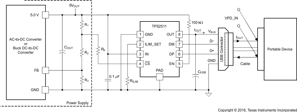 Figure 12. TPS2511 Charging System Schematic Diagram
The charging current of most portable devices is less than their maximum charging current while VPD_IN is less than the certain voltage value. Furthermore, actual charging current of PD decreases with input voltage falling. Therefore, a portable devices cannot accomplish a fast charge with its maximum charging rated current if VBUS voltage drop across the power path is not compensated at the high charging current. The TPS2511 provides CS pin to report the high charging current for USB chargers to increase the 5-VOUT voltage. This is shown by the solid lines of Figure 13.
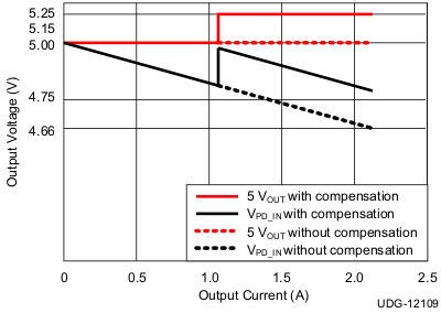 Figure 13. TPS2511 CS Function
Equation 2 through Equation 5 refer to Figure 12.
The power supply output voltage is calculated in Equation 2.

5 VOUT and VFB are known. If R3 is given and R1 is fixed, R2 can be calculated. The 5 VOUT voltage change with compensation is shown in Equation 3 and Equation 4.


If R1 is less than R3, then Equation 4 can be simplified as Equation 5.

7.3.8 Divide Mode Selection of 5-W and 10-W USB Chargers
The TPS2511 provides two types of connections between the DP pin and the DM pin and between the D+ data line and the D– data line of the USB connector for a 5-W USB charger and a 10-W USB charger with a single USB port. For a 5-W USB charger, the DP pin is connectd to the D– line and the DM pin is connected to the D+ line. This is shown in Figure 16 and Figure 17. It is necessary to apply DP and DM to D+ and D– of USB connector for 10-W USB chargers. See Figure 14 and Figure 15. Table 2 shows different charging schemes for both 5-W and 10-W USB charger solutions
Table 2. Charging Schemes for 5-W and 10-W USB Chargers
| USB CHARGER TYPE | CONTAINING CHARGING SCHEMES | ||
|---|---|---|---|
| 5-W | Divider1 | 1.2 V on both D+ and D– Lines | BC1.2 DCP |
| 10-W | Divider2 | 1.2 V on both D+ and D– Lines | BC1.2 DCP |
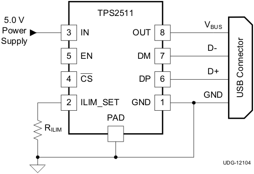 Figure 14. 10-W USB Charger Application With Power Switch
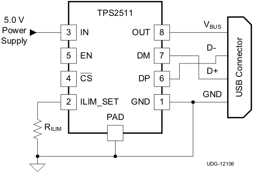 Figure 16. 5-W USB Charger Application With Power Switch
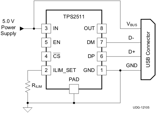 Figure 15. 10-W USB Charger Application Without Power Switch
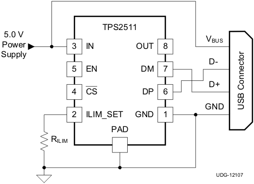 Figure 17. 5-W USB Charger Application Without Power Switch
7.4 Device Functional Modes
7.4.1 Dedicated Charging Port (DCP)
A dedicated charging port (DCP) is a downstream port on a device that outputs power through a USB connector, but is not capable of enumerating a downstream device, which generally allows portable devices to fast charge at their maximum rated current. A USB charger is a device with a DCP, such as a wall adapter or car power adapter. A DCP is identified by the electrical characteristics of its data lines. The following DCP identification circuits are usually used to meet the handshaking detections of different portable devices.
7.4.1.1 Short the D+ Line to the D– Line
The USB BC1.2 Specification and the Chinese Telecommunications Industry Standard YD/T 1591-2009 define that the D+ and D– data lines must be shorted together with a maximum series impedance of 200 Ω. This is shown in Figure 18.
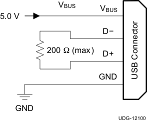 Figure 18. DCP Short Mode
7.4.1.2 Divider1 (DCP Applying 2 V on D+ Line and 2.7 V on D– Line) or Divider2 (DCP Applying 2.7 V on D+ Line and 2 V on D– Line)
There are two charging schemes for divider DCP. They are named after Divider1 and Divider2 DCPs that are shown in Figure 19 and Figure 20. The Divider1 charging scheme is used for 5-W adapters, Divider1 applies 2 V to the D+ line and 2.7 V to the D– data line. The Divider2 charging scheme is used for 10-W adapters and applies 2.7 V on the D+ line and 2 V is applied on the D– line.
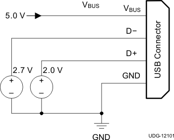 Figure 19. Divider1 DCP
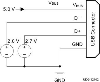 Figure 20. Divider2 DCP
7.4.1.3 Applying 1.2 V to the D+ Line and 1.2 V to the D– Line
As shown in Figure 21, some tablet USB chargers require 1.2 V on the shorted data lines of the USB connector. The maximum resistance between the D+ line and the D– line is 200 Ω.
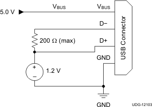 Figure 21. DCP Applying 1.2 V to the D+ Line and 1.2 V to the D– Line
The TPS2511 is a combination of a current-limiting USB power switch and an USB DCP identification controller. Applications include vehicle power charger, wall adapters with USB DCP and other USB chargers. The TPS2511 DCP controller has the auto-detect feature that monitors the D+ and D– line voltages of the USB connector, providing the correct electrical characteristics on the DP and DM pins for the correct detections of compliant portable devices to fast charge. These portable devices include smart phones, 5-V tablets, and personal media players.
The TPS2511 power-distribution switch is intended for applications where heavy capacitive loads and short circuits are likely to be encountered, incorporating a 70-mΩ, N-channel MOSFET in a single package. This device provides hiccup mode when in current limit and OUT voltage is less than 3.8 V (typical) or an over-temperature protection occurs under an overload condition. Hiccup mode operation can reduce the output short-circuit current down to several milliamperes. The TPS2511 provides a logic-level enable EN pin to control the device turnon and turnoff and an open-drain output CS for compensating VBUS to account for cable I × R voltage loss.
7.4.2 DCP Auto-Detect
The TPS2511 integrates an auto-detect feature to support divider mode, short mode and 1.2 V / 1.2 V mode. If a divider device is attached, 2.7 V is applied to the DP pin and 2 V is applied to the DM pin. If a BC1.2-compliant device is attached, the TPS2511 automatically switches into short mode. If a device compliant with the 1.2 V / 1.2 V charging scheme is attached, 1.2 V is applied on both the DP pin and the DM pin. The functional diagram of DCP auto-detect feature is shown in Figure 22.
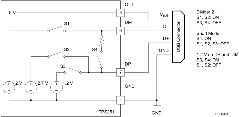 Figure 22. TPS2511 DCP Auto-Detect Functional Diagram