ZHCS981A JUNE 2012 – August 2016 TPS2511
PRODUCTION DATA.
- 1 特性
- 2 应用范围
- 3 说明
- 4 修订历史记录
- 5 Pin Configuration and Functions
- 6 Specifications
-
7 Detailed Description
- 7.1 Overview
- 7.2 Functional Block Diagram
- 7.3
Feature Description
- 7.3.1 Overcurrent Protection
- 7.3.2 Current Limit Threshold
- 7.3.3 Current-Sensing Report (CS)
- 7.3.4 Undervoltage Lockout (UVLO) and Enable (EN)
- 7.3.5 Soft Start, Reverse Blocking, and Discharge Output
- 7.3.6 Thermal Sense
- 7.3.7 VBUS Voltage Drop Compensation
- 7.3.8 Divide Mode Selection of 5-W and 10-W USB Chargers
- 7.4 Device Functional Modes
- 8 Application and Implementation
- 9 Power Supply Recommendations
- 10Layout
- 11器件和文档支持
- 12机械、封装和可订购信息
8 Application and Implementation
NOTE
Information in the following applications sections is not part of the TI component specification, and TI does not warrant its accuracy or completeness. TI’s customers are responsible for determining suitability of components for their purposes. Customers should validate and test their design implementation to confirm system functionality.
8.1 Application Information
The TPS2511 is a USB-dedicated charging-port controller and power switch with cable compensation. It is typically used for wall adapter or power bank as a USB charging controller and overcurrent protector.
8.2 Typical Application
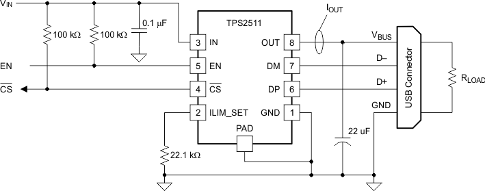 Figure 23. Test Circuit for System Operation
8.2.1 Design Requirements
For this design example, request IOS; Minimum must exceed 2100 mA.
When choosing the power switch, TI recommends following these general steps:
- Determine the voltage of the power rail, 3.3 V or 5 V, and then choose the operation range of power switch can cove power rail.
- Determine the normal operation current; for example, the maximum allowable current drawn by portable equipment for USB 2.0 port is 500 mA, so the normal operation current is 500 mA and the minimum current limit of power switch must exceed 500 mA to avoid false trigger during normal operation.
- Determine the maximum allowable current provided by up-stream power, and then decide the maximum current limit of power switch that must lower it to ensure power switch can protect the up-stream power when overload is encountered at the output of power switch.
NOTE
Choosing power switch with tighter current limit tolerance can loosen the up-stream power supply design.
8.2.2 Detailed Design Procedure
The user-programmable RILIM resistor on the ILIMIT_SET pin sets the current limit. The TPS2511 uses an internal regulation loop to provide a regulated voltage on the ILIM_SET pin. The current limiting threshold is proportional to the current sourced out of the ILIM_SET pin. The recommended 1% resistor range for RILIM is from 16.9 kΩ to 750 kΩ to ensure stability of the internal regulation loop, although not exceeding 210 kΩ results in a better accuracy. Many applications require that the minimum current limit remain above a certain current level or that the maximum current limit remain below a certain current level, so it is important to consider the tolerance of the overcurrent threshold when selecting a value for RILIM. Equation 6 and Equation 7 calculate the resulting overcurrent thresholds for a given external resistor value (RILIM). The traces routing the RILIM resistor to the TPS2511 must be as short as possible to reduce parasitic effects on the current limit accuracy. The equations along with Figure 24 and Figure 25 can be used to estimate the minimum and maximum variation of the current limit threshold for a predefined resistor value. This variation disregards the inaccuracy of the resistor itself.

where
- IOS_MIN is in mA
- RILIM is in kΩ
xxxxxx

where
- IOS_MAX is in mA
- RILIM is in kΩ
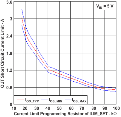
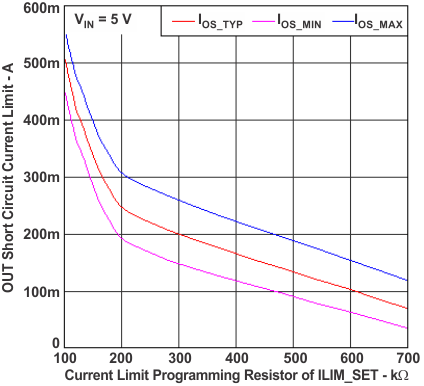
For this example design, as shown in Equation 8, IOS_MIN = 2100 mA.


Including resistor tolerance, target nominal resistance value given by Equation 10.

Choose Equation 11.
8.2.2.1 Input and Output Capacitance
Input and output capacitance improves the performance of the device; the actual capacitance must be optimized for the particular application. For all applications, TI recommends placing a 0.1-µF or greater ceramic bypass capacitor between IN and GND, as close to the device as possible for local noise decoupling. This precaution reduces ringing on the input due to power-supply transients. Additional input capacitance may be needed on the input to reduce voltage undershoot from exceeding the UVLO of other load share one power rail with TPS2511 or overshoot from exceeding the absolute-maximum voltage of the device during heavy transient conditions. This is especially important during bench testing when long, inductive cables are used to connect the evaluation board to the bench power supply.
TI recommends placing at least a 22-µF ceramic capacitor or higher-value electrolytic capacitor on the output pin when large transient currents are expected on the output to reduce the undershoot, which is caused by the inductance of the output power bus just after a short has occurred and the TPS2511 has abruptly reduced OUT current. Energy stored in the inductance drives the OUT voltage down and potentially negative as it discharges.
8.2.3 Application Curves
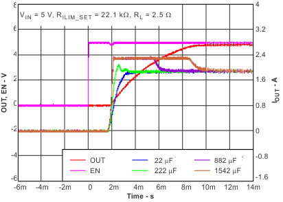 Figure 26. Inrush Current With Different Capacitance Load
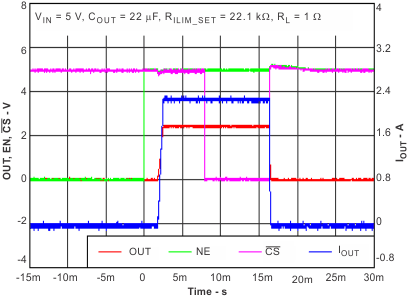 Figure 28. Enable into 1-Ω Load
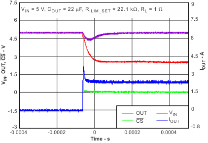 Figure 30. 1-Ω Load Applied
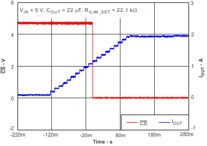 Figure 32. Output Current-Sensing Report
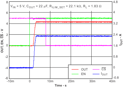 Figure 27. Enable into 1.83-Ω Load
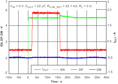 Figure 29. Enable into Short
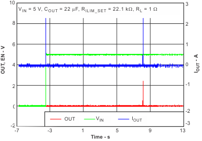 Figure 31. Hiccup Mode While Enabled into 1-Ω Load