SLVSBY8D May   2013  – June 2020 TPS2513 , TPS2513A , TPS2514 , TPS2514A

PRODUCTION DATA.  

  1. Features
  2. Applications
  3. Description
    1.     Device Images
      1.      Simplified Schematic
  4. Revision History
  5. Device Options
  6. Pin Configuration and Functions
    1.     Pin Functions: TPS2513x
    2.     Pin Functions: TPS2514x
  7. Specifications
    1. 7.1 Absolute Maximum Ratings
    2. 7.2 ESD Ratings
    3. 7.3 Recommended Operating Conditions
    4. 7.4 Thermal Information
    5. 7.5 Electrical Characteristics
    6. 7.6 Typical Characteristics
  8. Detailed Description
    1. 8.1 Overview
    2. 8.2 Functional Block Diagrams
    3. 8.3 Feature Description
      1. 8.3.1 Dedicated Charging Port (DCP)
      2. 8.3.2 Short the D+ Line to the D– Line
      3. 8.3.3 Divider DCP
      4. 8.3.4 Applying 1.2 V to the D+ Line and 1.2 V to the D– Line
      5. 8.3.5 DCP Auto-Detect
      6. 8.3.6 Undervoltage Lockout (UVLO)
    4. 8.4 Device Functional Modes
  9. Applications and Implementation
    1. 9.1 Application Information
    2. 9.2 Typical Applications
      1. 9.2.1 Design Requirements
      2. 9.2.2 Detailed Design Procedure
        1. 9.2.2.1 Divide Mode Selection of 5-W and 10-W USB Chargers
      3. 9.2.3 Application Curves
  10. 10Power Supply Recommendations
  11. 11Layout
    1. 11.1 Layout Guidelines
    2. 11.2 Layout Example
  12. 12Device and Documentation Support
    1. 12.1 Related Links
    2. 12.2 Receiving Notification of Documentation Updates
    3. 12.3 Support Resources
    4. 12.4 Trademarks
    5. 12.5 Electrostatic Discharge Caution
    6. 12.6 Glossary
  13. 13Mechanical, Packaging, and Orderable Information

封装选项

机械数据 (封装 | 引脚)
散热焊盘机械数据 (封装 | 引脚)
订购信息

Short the D+ Line to the D– Line

The USB BC1.2 Specification and the Chinese Telecommunications Industry Standard YD/T 1591-2009 define that the D+ and D– data lines must be shorted together with a maximum series impedance of 200 Ω. This is shown in Figure 10.
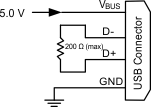
TPS2513 TPS2513A TPS2514 TPS2514A fig009_lvsby8.gifFigure 10. DCP Short Mode