ZHCSDG1 March   2015 TPS25200-Q1

PRODUCTION DATA.  

  1. 特性
  2. 应用范围
  3. 说明
  4. 简化电路原理图
  5. 修订历史记录
  6. Pin Configuration and Functions
  7. Specifications
    1. 7.1 Absolute Maximum Ratings
    2. 7.2 ESD Ratings
    3. 7.3 Recommended Operating Conditions
    4. 7.4 Thermal Information
    5. 7.5 Electrical Characteristics
    6. 7.6 Switching Characteristics
    7. 7.7 Typical Characteristics
  8. Parameter Measurement Information
  9. Detailed Description
    1. 9.1 Overview
    2. 9.2 Functional Block Diagram
    3. 9.3 Feature Description
      1. 9.3.1 Enable
      2. 9.3.2 Thermal Sense
      3. 9.3.3 Overcurrent Protection
      4. 9.3.4 FAULT Response
      5. 9.3.5 Output Discharge
    4. 9.4 Device Functional Modes
      1. 9.4.1 Undervoltage Lockout (UVLO)
      2. 9.4.2 Overcurrent Protection (OCP)
      3. 9.4.3 Overvoltage Clamp (OVC)
      4. 9.4.4 Overvoltage Lockout (OVLO)
  10. 10Application and Implementation
    1. 10.1 Application Information
    2. 10.2 Typical Application
      1. 10.2.1 Overvoltage and Overcurrent Protector
        1. 10.2.1.1 Design Requirements
        2. 10.2.1.2 Detailed Design Procedure
          1. 10.2.1.2.1 Step by Step Design Produce
          2. 10.2.1.2.2 Input and Output Capacitance
          3. 10.2.1.2.3 Programming the Current-Limit Threshold
          4. 10.2.1.2.4 Design Above a Minimum Current Limit
          5. 10.2.1.2.5 Design Below a Maximum Current Limit
          6. 10.2.1.2.6 Power Dissipation and Junction Temperature
        3. 10.2.1.3 Application Curves
  11. 11Power Supply Recommendations
  12. 12Layout
    1. 12.1 Layout Guidelines
    2. 12.2 Layout Example
  13. 13器件和文档支持
    1. 13.1 文档支持
      1. 13.1.1 相关文档 
    2. 13.2 商标
    3. 13.3 静电放电警告
    4. 13.4 术语表
  14. 14机械封装和可订购信息

封装选项

机械数据 (封装 | 引脚)
散热焊盘机械数据 (封装 | 引脚)
订购信息

12 Layout

12.1 Layout Guidelines

  • For all applications, a 0.1-µF or greater ceramic bypass capacitor between the IN and GND pins is recommended as close to the device as possible for local noise decoupling.
  • For output capacitance, see Figure 16. A low-ESR ceramic capacitor is recommended.
  • The traces routing the RILIM resistor to the device should be as short as possible to reduce parasitic effects on the current-limit accuracy.
  • The thermal pad should be directly connected to PCB ground plane using wide and short copper trace.

12.2 Layout Example
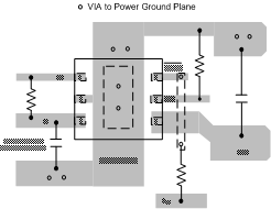
TPS25200-Q1 layout_slvscu5.gifFigure 32. TPS25200-Q1 Board Layout