ZHCSGL1A May 2017 – May 2017 TPS2547
PRODUCTION DATA.
- 1 特性
- 2 应用
- 3 说明
- 4 修订历史记录
- 5 Pin Configuration and Functions
- 6 Specifications
- 7 Parameter Measurement Information
-
8 Detailed Description
- 8.1 Overview
- 8.2 Functional Block Diagram
- 8.3
Feature Description
- 8.3.1 Standard Downstream Port (SDP) USB 2.0/USB 3.0
- 8.3.2 Charging Downstream Port (CDP)
- 8.3.3 Dedicated Charging Port (DCP)
- 8.3.4 Wake on USB Feature (Mouse/Keyboard Wake Feature)
- 8.3.5 Load Detect
- 8.3.6 Power Wake
- 8.3.7 Port Power Management (PPM)
- 8.3.8 Overcurrent Protection
- 8.3.9 FAULT Response
- 8.3.10 Undervoltage Lockout (UVLO)
- 8.3.11 Thermal Sense
- 8.4 Device Functional Modes
- 9 Application and Implementation
- 10Power Supply Recommendations
- 11Layout
- 12器件和文档支持
- 13机械、封装和可订购信息
9 Application and Implementation
NOTE
Information in the following applications sections is not part of the TI component specification, and TI does not warrant its accuracy or completeness. TI’s customers are responsible for determining suitability of components for their purposes. Customers must validate and test their design implementation to confirm system functionality.
9.1 Application Information
Power-on-reset (POR) holds device in initial state while output is held in discharge mode. Any POR event returns the device to initial state. After POR clears, device goes to the next state depending on the CTL lines as shown in Figure 38.
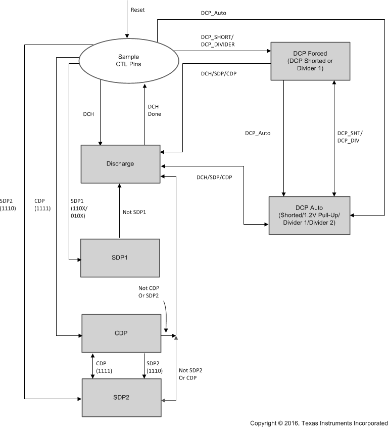 Figure 38. TPS2547 Charging States
9.1.1 Output Discharge
To allow a charging port to renegotiate current with a portable device, the TPS2547 device uses the OUT discharge function. The device proceeds by turning off the power switch while discharging OUT. The device then turns on the power switch again to reassert the OUT voltage. This discharge function is automatically applied, as shown in Figure 26. There are two discharge times, tDCHG_L and tDCHG_S. tDCHG_L is from SDP1/SDP2/CDP to DCP_Auto, and tDCHG_S is from DCP_Auto to SDP1/SDP2/CDP.
9.2 Typical Application
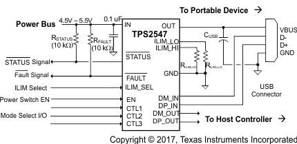 Figure 39. Typical Application Schematic USB Port Charging
9.2.1 Design Requirements
For this design example, use the parameters listed in Table 4.
Table 4. Design Parameters
| DESIGN PARAMETER | EXAMPLE VALUE | ||
|---|---|---|---|
| Input voltage, V(IN) | 5 V | ||
| Output voltage, V(DC) | 5 V | ||
| Maximum continuous output current, I(OUT) | 2.5 A | ||
| Current limit, I(LIM_LO) at RILIM_LO = 80.6 kΩ | 0.625 A | ||
| Current Limit, I(LIM_HI) at RILIM_HI = 16.9 kΩ | 2.97 A |
9.2.2 Detailed Design Procedure
9.2.2.1 Current-Limit Settings
The TPS2547 has two independent current limit settings that are each programmed externally with a resistor. The ILIM_HI setting is programmed with RILIM_HI connected between ILIM_HI and GND. The ILIM_LO setting is programmed with RILIM_LO connected between ILIM_LO and GND. Consult the Device Truth Table (Table 3) to see when each current limit is used. Both settings have the same relation between the current limit and the programming resistor.
RILIM_LO is optional and the ILIM_LO pin may be left unconnected if the following conditions are met:
- ILIM_SEL is always set high
- Load Detection - Port Power Management is not used
Equation 1 programs the typical current limit:
RILIM_XX corresponds to either RILIM_HI or RILIM_LO as appropriate.
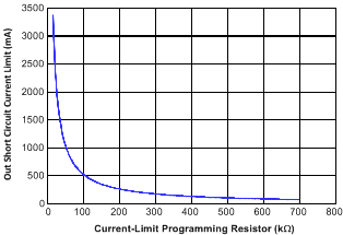
Many applications require that the current limit meet specific tolerance limits. When designing to these tolerance limits, both the tolerance of the TPS2547 current limit and the tolerance of the external programming resistor must be taken into account. The following equations approximate the TPS2547 minimum and maximum current limits to within a few mA, and are appropriate for design purposes. The equations do not constitute part of Texas Instrument's published device specifications for purposes of Texas Instrument's product warranty. These equations assume an ideal - no variation - external programming resistor. To take resistor tolerance into account, first determine the minimum and maximum resistor values based on its tolerance specifications, and use these values in the equations. Because of the inverse relation between the current limit and the programming resistor, use the maximum resistor value in the Equation 2 and the minimum resistor value in the Equation 3.
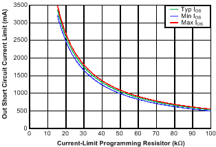 Figure 41. Current Limit Setting vs Programming Resistor
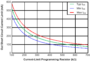 Figure 42. Current Limit Setting vs Programming Resistor
The traces routing the RILIM_XX resistors must be a sufficiently low resistance as to not affect the current-limit accuracy. The ground connection for the RILIM_XX resistors is also very important. The resistors need to reference back to the TPS2547 GND pin. Follow normal board layout practices to ensure that current flow from other parts of the board does not impact the ground potential between the resistors and the TPS2547 GND pin.
9.2.3 Application Curves
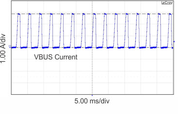 Figure 43. High-Current Limit
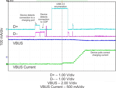
CDP (CTL1 = CTL2 = CTL3 = ILIM_SEL = 1)
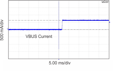 Figure 44. Low-Current Limit


