ZHCSGL1A May 2017 – May 2017 TPS2547
PRODUCTION DATA.
- 1 特性
- 2 应用
- 3 说明
- 4 修订历史记录
- 5 Pin Configuration and Functions
- 6 Specifications
- 7 Parameter Measurement Information
-
8 Detailed Description
- 8.1 Overview
- 8.2 Functional Block Diagram
- 8.3
Feature Description
- 8.3.1 Standard Downstream Port (SDP) USB 2.0/USB 3.0
- 8.3.2 Charging Downstream Port (CDP)
- 8.3.3 Dedicated Charging Port (DCP)
- 8.3.4 Wake on USB Feature (Mouse/Keyboard Wake Feature)
- 8.3.5 Load Detect
- 8.3.6 Power Wake
- 8.3.7 Port Power Management (PPM)
- 8.3.8 Overcurrent Protection
- 8.3.9 FAULT Response
- 8.3.10 Undervoltage Lockout (UVLO)
- 8.3.11 Thermal Sense
- 8.4 Device Functional Modes
- 9 Application and Implementation
- 10Power Supply Recommendations
- 11Layout
- 12器件和文档支持
- 13机械、封装和可订购信息
11 Layout
11.1 Layout Guidelines
For the trace routing of DP_IN, DM_IN, DP_OUT, and DM_OUT: route these traces as micro-strips with nominal differential impedance of 90 Ω. Minimize the use of vias in the high-speed data lines. Keep the reference GND plane devoid from cuts or splits above the differential pairs to prevent impedance discontinuities. For more information, see the High-Speed USB Platform Design Guidelines from Intel.
The trace routing from the upstream regulator to the TPS2547 IN pin must be as short as possible to reduce voltage drop and parasitic inductance.
In order to meet IEC61000-4-2 level 4 ESD, external circuitry is required. Refer to the guidelines provided in the 相关文档 section.
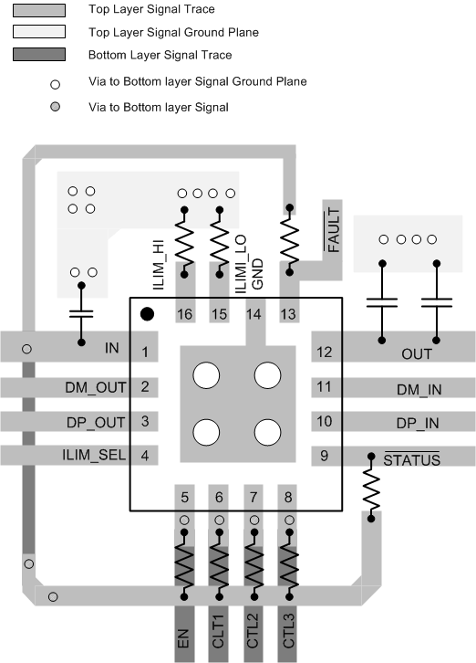
The traces routing from the RILIM_HI and RILIM_LO resistors to the device must be as short as possible to reduce parasitic effects on the current-limit accuracy.
The thermal pad must be directly connected to the PCB ground plane using wide and short copper trace.
11.2 Layout Example
 Figure 46. Layout Recommendation