ZHCSFL0 September 2016 TPS2549
PRODUCTION DATA.
- 1 特性
- 2 应用
- 3 说明
- 4 修订历史记录
- 5 Pin Configuration and Functions
- 6 Specifications
- 7 Parameter Measurement Information
-
8 Detailed Description
- 8.1 Overview
- 8.2 Functional Block Diagram
- 8.3 Feature Description
- 8.4 Device Functional Modes
- 9 Application and Implementation
- 10Power Supply Recommendations
- 11Layout
- 12器件和文档支持
- 13机械、封装和可订购信息
9 Application and Implementation
NOTE
Information in the following applications sections is not part of the TI component specification, and TI does not warrant its accuracy or completeness. TI’s customers are responsible for determining suitability of components for their purposes. Customers should validate and test their design implementation to confirm system functionality.
9.1 Application Information
The TPS2549 device is a USB charging-port controller and power switch with cable compensation. It is typically used for USB port protection and as a USB charging controller. The following design procedure can be used to select components for the TPS2549 device. This section presents a simplified discussion of how to design cable compensation.
9.2 Typical Application
USB port charging requires a voltage regulator to convert battery voltage to 5-V VBUS output. Because the VBUS, D+, and D– pins of a USB port are exposed, there is a need for a protection device that has VBUS overcurrent and D+ and D– ESD protection. An additional need is a charging controller with integrated CDP and DCP charging protocols on D+ and D– to support fast charging. A schematic of an application circuit with cable compensation is shown in Figure 49. An LMR14030 device is used as the voltage regulator, and the TPS2549 device is used as the charging controller with protection features.
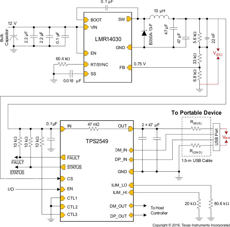 Figure 49. Typical Application Schematic: USB Port Charging With Cable Compensation
9.2.1 Design Requirements
For this design example, use the following as the input parameters.
| DESIGN PARAMETER | EXAMPLE VALUE |
|---|---|
| Input voltage, V(IN) | 12 V |
| Output voltage, V(DC) | 5 V |
| Total parasitic resistance including TPS2549 rDS(on) | 420 mΩ |
| Maximum continuous output current, I(OUT) | 2.4 A |
| Current limit, I(LIM) | 2.5 A to 2.9 A |
9.2.2 Detailed Design Procedure
To begin the design process, a few parameters must be decided upon. The designer needs to know the following:
- Total resistance including power switch rDS(on), cable resistance, and the contact resistance of connectors
- The maximum continuous output current for the charging port. The minimum current-limit setting of TPS2549 device must be higher than this current.
- The maximum output current of the upstream dc-dc converter. The maximum current-limit setting of TPS2549 device must be lower than this current.
9.2.2.1 Input and Output Capacitance
Input and output capacitance improves the performance of the device; the actual capacitance should be optimized for the particular application. All protection circuits including the TPS2549 device have the potential for input voltage droop, overshoot, and output-voltage undershoot.
For all applications, TI recommends a 0.1-µF or greater ceramic bypass capacitor between IN and GND, placed as close as possible to the device for the local noise decoupling.
The TPS2549 device is used for 5-V power rail protection when a hot-short occurs on the output or when plugging in a capacitive load. Due to the limited response time of the upstream power supply, a large load transient can deplete the charge on the output capacitor of the power supply, causing a voltage droop. If the power supply is shared with other loads, ensure that voltage droop from current surges of the other loads do not force the TPS2549 device into UVLO. Increasing the upstream power supply output capacitor can reduce this droop. Shortening the connection impedance (resistance and inductance) between the TPS2549 device and the upstream power supply can also help reduce the voltage droop and overshoot on the TPS2549 input power bus.
Input voltage overshoots can be caused by either of two effects. The first cause is an abrupt application of input voltage in conjunction with input power-bus inductance and input capacitance when the IN terminal is in the high-impedance state (before turnon). Theoretically, the peak voltage is 2 times the applied voltage. The second cause is due to the abrupt reduction of output short-circuit current when the TPS2549 device turns off and energy stored in the input inductance drives the input voltage high. Applications with large input inductance (for example, connecting the evaluation board to the bench power supply through long cables) may require large input capacitance to prevent the voltage overshoot from exceeding the absolute maximum voltage of the device.
For output capacitance, consider the following three application situations.
The first, output voltage undershoot is caused by the inductance of the output power bus just after a short has occurred and the TPS2549 has abruptly reduced OUT current. Energy stored in the inductance will drive the OUT voltage down and potentially negative as it discharges. Applications with large output inductance (such as from a cable) benefit from use of a high-value output capacitor to control the voltage undershoot. Second, for USB-port application, because the OUT pin is exposed to the air, the application must withstand ESD stress without damage. Because there is no internal IEC ESD cell as on DP_IN and DM_IN, using a low-ESR capacitance can make this pin robust. Third, when plugging in apacitive load such as the input capacitor of any portable device, having a large output capacitance can help reduce the peak current and up-stream power supply output voltage droop. So for TPS2549 output capacitance, recommended practice is typically adding two 47-µF ceramic capacitors.
9.2.2.2 Cable Compensation Calculation
Based on the known total resistance, Table 4 shows the calculation.
Table 4. Cable Compensation Calculation
| CALCULATION EQUATION(1) | CALCULATED VALUE | ASSEMBLY VALUE | |
|---|---|---|---|
| V(DC) (V) without load | 5 | ||
| R(G) (kΩ) | 6.8 | 6.8 | |
| R(total) (Ω) | 0.42 | ||
| G(CS) (mA/A) | 0.075 | ||
| R(FA) (kΩ) | R(FA) = R(total) / G(CS) | 5.6 | 5.6 |
| V(FB) (V) | 0.75 | ||
| R(FB) (kΩ) | R(FB) = [V(DC) / (V(FB) / R(G))] – R(G) – R(FA) | 32.93 | 33 |
| V(CS) (V)(2) | VCS = (V(FB) / R(G)) × (R(G) + R(FB)) | 4.39 | |
| Maximum IOS (A) at 20 kΩ | 2.84 | ||
| V(DC,max) output (V)(3) | V(DC,max) = 5 + I(OS,max) × G(CS,max) × R(FA) | 6.25 | |
| C(OUT) (µF) | 2 × 47 | ||
| C(COMP) (nF)(4) | C(COMP) ≥ 3 × G(CS) × C(OUT) | ≥21.15 | 22 |
9.2.2.3 Power Dissipation and Junction Temperature
The low on-resistance of the N-channel MOSFET allows small surface-mount packages to pass large currents. It is good design practice to estimate power dissipation and junction temperature. The following analysis gives an approximation for calculating junction temperature based on the power dissipation in the package. However, it is important to note that thermal analysis is strongly dependent on additional system-level factors. Such factors include air flow, board layout, copper thickness and surface area, and proximity to other devices dissipating power. Good thermal design practice must include all system-level factors in addition to individual component analysis. Begin by determining the rDS(on) of the N-channel MOSFET relative to the input voltage and operating temperature. As an initial estimate, use the highest operating ambient temperature of interest and read rDS(on) from the typical characteristics graph. Using this value, the power dissipation can be calculated by:

where:
PD = Total power dissipation (W)
rDS(on) = Power-switch on-resistance (Ω)
IOUT = Maximum current-limit threshold (A)
This step calculates the total power dissipation of the N-channel MOSFET.
Finally, calculate the junction temperature:

where:
TA = Ambient temperature (°C)
RθJA = Thermal resistance (°C/W)
PD = Total power dissipation (W)
Compare the calculated junction temperature with the initial estimate. If they are not within a few degrees, repeat the calculation using the refined rDS(on) from the previous calculation as the new estimate. Two or three iterations are generally sufficient to achieve the desired result. The final junction temperature is highly dependent on thermal resistance RθJA, and thermal resistance is highly dependent on the individual package and board layout.
9.2.3 Application Curves
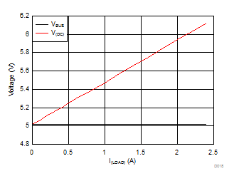
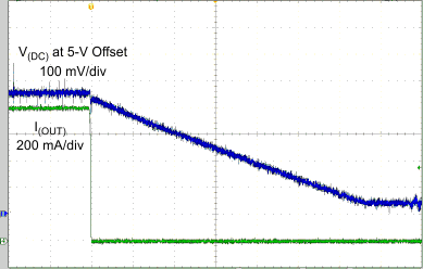
| t = 20 ms/div |
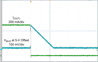
| t = 20 ms/div |
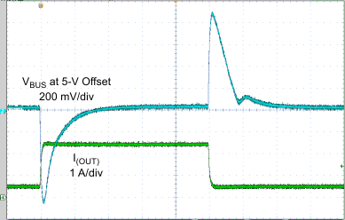
| t = 200 µs/div |
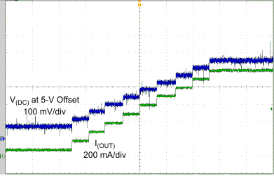
| t = 20 ms/div | ||

| t = 20 ms/div |
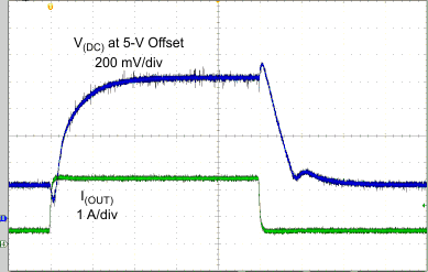
| t = 200 µs/div |
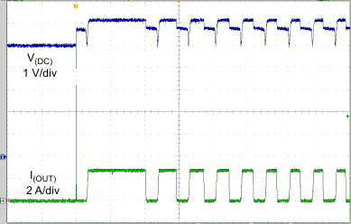
| t = 200 µs/div |