ZHCSFK7A September 2016 – October 2016 TPS254900-Q1
PRODUCTION DATA.
- 1 特性
- 2 应用范围
- 3 说明
- 4 修订历史记录
- 5 Pin Configuration and Functions
- 6 Specifications
- 7 Parameter Measurement Information
-
8 Detailed Description
- 8.1 Overview
- 8.2 Functional Block Diagram
- 8.3 Feature Description
- 8.4 Device Functional Modes
- 9 Application and Implementation
- 10Power Supply Recommendations
- 11Layout
- 12器件和文档支持
- 13机械、封装和可订购信息
9 Application and Implementation
NOTE
Information in the following applications sections is not part of the TI component specification, and TI does not warrant its accuracy or completeness. TI’s customers are responsible for determining suitability of components for their purposes. Customers should validate and test their design implementation to confirm system functionality.
9.1 Application Information
The TPS254900-Q1 device is a USB charging-port controller and power switch with cable compensation and short-to-battery protection for VBUS, D+, and D–. The device is typically used for automotive USB port protection and as a USB charging controller. The following design procedure can be used to select components for the TPS254900-Q1. This section presents a simplified discussion of how to choose external components for VBUS, D+, and D– short-to-battery protection. For cable-compensation design information, see the data sheet (SLUSCE3) for the TPS2549-Q1 device, which has features and design considerations very similar to those of the TPS254900-Q1 device.
9.2 Typical Application
For an automotive USB charging port, the VBUS, D+, and D– pins are exposed and require a protection device. The protection required includes VBUS overcurrent, D+ and D– ESD protection, and short-to-battery protection. This charging-port device protects the upstream dc-dc converter (bus line) and automotive SOC or hub chips (D+ and D– data lines). An application schematic of this circuit with short-to-battery protection is shown in Figure 43.
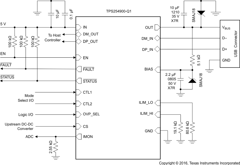 Figure 43. Typical Application Schematic: USB Port Charging With Cable Compensation
9.2.1 Design Requirements
For this design example, use the following as the input parameters.
| DESIGN PARAMETER | EXAMPLE VALUE |
|---|---|
| Battery voltage, V(BAT) | 18 V |
| Short-circuit cable | 0.5 m |
9.2.2 Detailed Design Procedure
To begin the design process, the designer must know the following:
- The battery voltage
- The short-circuit cable length
- The maximum continuous output current for the charging port. The minimum current-limit setting of TPS254900-Q1 device must be higher than this current.
- The maximum output current of the upstream dc-dc converter. The maximum current-limit setting of TPS254900-Q1 device must be lower than this current.
- For cable compensation, the total resistance including power switch rDS(on), cable resistance, and connector contact resistance must be specified.
9.2.2.1 Input Capacitance
Consider the following application situations when choosing the input capacitors.
For all applications, TI recommends a 0.1-µF or greater ceramic bypass capacitor between IN and GND, placed as close as possible to the device for local noise decoupling.
During output short or hot plug-in of a capacitive load, high current flows through the TPS254900-Q1 device back to the upstream dc-dc converter until the TPS254900-Q1 device responds (after t(IOS)). During this response time, the TPS254900-Q1 input capacitance and the dc-dc converter output capacitance source current to keep VIN above the UVLO of the TPS254900-Q1 device and any shared circuits. Size the input capacitance for the expected transient conditions and keep the path between the TPS254900-Q1 device and the dc-dc converter short to help minimize voltage drops.
Input voltage overshoots can be caused by either of two effects. The first cause is an abrupt application of input voltage in conjunction with input power-bus inductance and input capacitance when the IN pin is in the high-impedance state (before turnon). Theoretically, the peak voltage is 2 times the applied voltage. The second cause is due to the abrupt reduction of output short-circuit current when the TPS254900-Q1 device turns off and energy stored in the input inductance drives the input voltage high. Applications with large input inductance (for example, a connection between the evaluation board and the bench power supply through long cables) may require large input capacitance to prevent the voltage overshoot from exceeding the absolute-maximum voltage of the device.
During the short-to-battery (EN = HIGH) condition, the input voltage follows the output voltage until OVP protection is triggered (t(OV_OUT)). After the TPS254900-Q1 device responds and turns off the power switch, the stored energy in the input inductance can cause ringing.
Based on the three situations described, 10-µF and 0.1-µF low-ESR ceramic capacitors, placed close to the input, are recommended.
9.2.2.2 Output Capacitance
Consider the following application situations when choosing the output capacitors.
After an output short occurs, the TPS254900-Q1 device abruptly reduces the OUT current, and the energy stored in the output power-bus inductance causes voltage undershoot and potentially reverse voltage as it discharges.
Applications with large output inductance (such as from a cable) benefit from the use of a high-value output capacitor to control the voltage undershoot.
For USB port applications, because the VBUS pin is exposed to IEC61000-4-2 level-4 ESD, use a low-ESR capacitance to protect OUT.
The TPS254900-Q1 device is capable of handling up to 18-V battery voltage. When VBUS is shorted to the battery, the LCR tank circuit formed can induce ringing. The peak voltage seen on the OUT pin depends on the short-circuit cable length. The parasitic inductance and resistance varies with length, causing the damping factor and peak voltage to differ. Longer cables with larger resistance reduce the peak current and peak voltage. Consider high-voltage derating for the ceramic capacitor, because the peak voltage can be higher than twice the battery voltage.
Based on the three situations described, a 10-µF, 35-V, X7R, 1210 low-ESR ceramic capacitor placed close to OUT is recommended. If the battery voltage is 16 V and a 16-V transient voltage suppressor (TVS) is used, then the capacitor voltage can be reduced to 25 V. Considering temperature variation, placing an additional 35-V aluminum electrolytic capacitor can lower the peak voltage and make the system more robust.
9.2.2.3 BIAS Capacitance
The capacitance on the BIAS pin helps the IEC ESD performance on the DM_IN and DP_IN pins.
When a short to battery on DP_IN, DM_IN and/or OUT occurs, high voltage can be seen on the BIAS pin. Place a 2.2-µF, 50-V, X7R, 0805, low-ESR ceramic capacitor close to the BIAS pin. The whole current path from BIAS to GND should be as short as possible. Additionally, use a 5.1-kΩ discharge resistor from BIAS to OUT.
9.2.2.4 Output and BIAS TVS
The TPS254900-Q1 device can withstand high transient voltages due to LCR tank ringing, but in order to make OUT, DP_IN, and DM_IN robust, place one TVS close to the OUT pin, and another TVS close to the BIAS pin. When choosing the TVS, the reverse standoff voltage VR depends on the battery voltage (16 V or 18 V). Considering the peak pulse power capability, a 400-W device is recommended such as an SMAJ16 for a 16-V battery or an SMAJ18 for an 18-V battery.
9.2.3 Application Curves
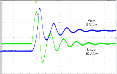
| VBAT = 14 V | t = 10 µs/div |
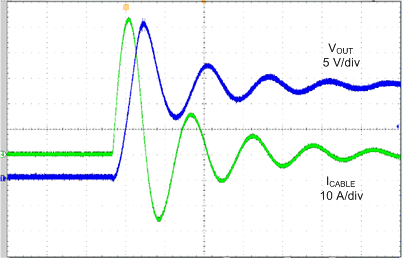
| VBAT = 18 V | t = 10 µs/div |
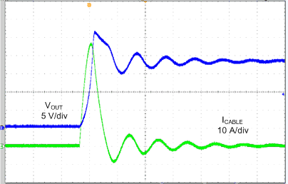
| t = 10 µs/div |
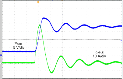
| t = 10 µs/div |
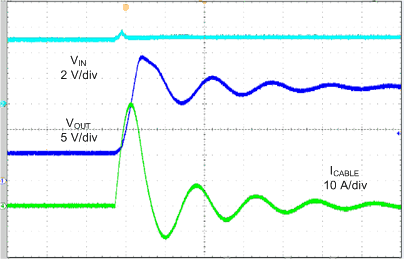
| t = 10 µs/div |
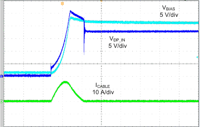
| RBIAS = 5.1 kΩ | t = 2 µs/div |
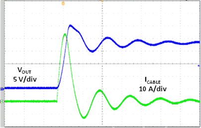
| t = 10 µs/div |
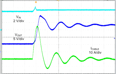
| t = 10 µs/div |
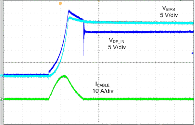
| RBIAS = 5.1 kΩ | t = 2 µs/div |
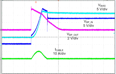
| R(BIAS) = 5.1 kΩ | t = 2 µs/div | R(DP_OUT) = 15 kΩ |