SLVS931B November 2009 – December 2016 TPS2556 , TPS2557
PRODUCTION DATA.
- 1 Features
- 2 Applications
- 3 Description
- 4 Revision History
- 5 Device Comparison Table
- 6 Pin Configuration and Functions
- 7 Specifications
- 8 Parameter Measurement Information
- 9 Detailed Description
-
10Application and Implementation
- 10.1 Application Information
- 10.2
Typical Applications
- 10.2.1 Current-Limiting Power-Distribution Switch
- 11Power Supply Recommendations
- 12Layout
- 13Device and Documentation Support
- 14Mechanical, Packaging, and Orderable Information
7 Specifications
7.1 Absolute Maximum Ratings
over operating free-air temperature range (unless otherwise noted)(1)(2)| MIN | MAX | UNIT | ||
|---|---|---|---|---|
| Voltage | IN, OUT, EN or EN, ILIM, and FAULT pins | –0.3 | 7 | V |
| Voltage from IN to OUT | –7 | 7 | V | |
| Continuous output current | Internally limited | |||
| Continuous FAULT sink current | 25 | mA | ||
| ILIM source current | Internally limited | |||
| Continuous total power dissipation | See Thermal Information | |||
| Maximum junction temperature | –40 | OTSD2 | °C | |
| Storage temperature, Tstg | -65 | 150 | °C | |
(1) Stresses beyond those listed under Absolute Maximum Ratings may cause permanent damage to the device. These are stress ratings only, which do not imply functional operation of the device at these or any other conditions beyond those indicated under Recommended Operating Conditions. Exposure to absolute-maximum-rated conditions for extended periods may affect device reliability.
(2) Voltages are referenced to GND unless otherwise noted.
7.2 ESD Ratings
| VALUE | UNIT | |||
|---|---|---|---|---|
| V(ESD) | Electrostatic discharge | Human-body model (HBM), per ANSI/ESDA/JEDEC JS-001(1) | ±2000 | V |
| Charged-device model (CDM), per JEDEC specification JESD22-C101(2) | ±500 | |||
| IEC 61000-4-2 contact discharge(3) | ±8000 | |||
| IEC 61000-4-2 air discharge(3) | ±15000 | |||
(1) JEDEC document JEP155 states that 500-V HBM allows safe manufacturing with a standard ESD control process.
(2) JEDEC document JEP157 states that 250-V CDM allows safe manufacturing with a standard ESD control process.
(3) Surges per EN61000-4-2, 1999 applied between USB and output ground of the TPS2556EVM (HPA423) evaluation module (see Using the TPS2556EVM-423 and TPS2557EVM-423). These were the test levels, not the failure threshold.
7.3 Recommended Operating Conditions
7.4 Thermal Information
| THERMAL METRIC(1) | TPS255x | UNIT | |
|---|---|---|---|
| DRB (VSON) | |||
| 8 PINS | |||
| RθJA | Junction-to-ambient thermal resistance | 41.5 | °C/W |
| RθJC(top) | Junction-to-case (top) thermal resistance | 54.5 | °C/W |
| RθJB | Junction-to-board thermal resistance | 16.4 | °C/W |
| ψJT | Junction-to-top characterization parameter | 0.7 | °C/W |
| ψJB | Junction-to-board characterization parameter | 16.6 | °C/W |
| RθJC(bot) | Junction-to-case (bottom) thermal resistance | 3.6 | °C/W |
(1) For more information about traditional and new thermal metrics, see the Semiconductor and IC Package Thermal Metrics application report.
7.5 Electrical Characteristics
over recommended operating conditions, VEN = 0 V or VEN = VIN (unless otherwise noted)(1)| PARAMETER | TEST CONDITIONS | MIN | TYP | MAX | UNIT | ||
|---|---|---|---|---|---|---|---|
| POWER SWITCH | |||||||
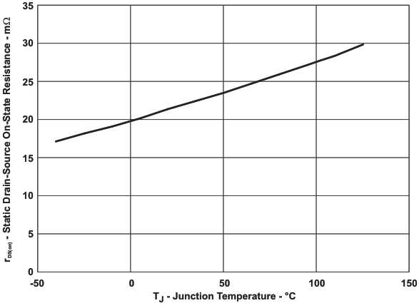
| rDS(ON) | Static drain-source on-state resistance | TJ = 25°C | 22 | 25 | mΩ | ||
| –40°C ≤TJ ≤ 125°C | 35 | ||||||
| Enable pin turn on and off threshold | 0.66 | 1.1 | V | ||||
| Enable input hysteresis(2) | 55 | mV | |||||
| IEN | Input current | VEN = 0 V or 6.5 V, VEN = 0 V or 6.5 V | –0.5 | 0.5 | µA | ||
| IOS | Current-limit threshold (Maximum DC output current IOUT delivered to load) and short-circuit current, OUT connected to GND | RILIM = 24.9 kΩ | 4130 | 4450 | 4695 | mA | |
| RILIM = 61.9 kΩ | 1590 | 1785 | 1960 | ||||
| RILIM = 100 kΩ | 935 | 1100 | 1260 | ||||
| IIN_OFF | Supply current, low-level output | VIN = 6.5 V, No load on OUT, VEN = 6.5 V or VEN = 0 V | 0.1 | 2 | µA | ||
| IIN_ON | Supply current, high-level output | VIN = 6.5 V, No load on OUT | RILIM = 24.9 kΩ | 95 | 120 | µA | |
| RILIM = 100 kΩ | 85 | 110 | µA | ||||
| IREV | Reverse leakage current | VOUT = 6.5 V, VIN = 0 V, TJ = 25 °C | 0.01 | 1 | µA | ||
| UVLO | Low-level input voltage (IN pin) | VIN rising | 2.35 | 2.45 | V | ||
| UVLO hysteresis (IN pin)(2) | 35 | mV | |||||
| FAULT FLAG | |||||||
| VOL | Output low voltage (FAULT pin) | IFAULT = 1 mA | 180 | mV | |||
| Off-state leakage | VFAULT = 6.5 V | 1 | µA | ||||
| FAULT deglitch | FAULT assertion or deassertion due to overcurrent condition | 6 | 9 | 13 | ms | ||
| THERMAL SHUTDOWN | |||||||
| OTSD2 | Thermal shutdown threshold | 155 | °C | ||||
| OTSD | Thermal shutdown threshold in current-limit | 135 | °C | ||||
| Hysteresis(2) | 20 | °C | |||||
(1) Pulse-testing techniques maintain junction temperature close to ambient temperature; thermal effects must be considered separately.
(2) These parameters are provided for reference only, and do no constitute part of TI's published specifications for purposes of TI's product warranty.
7.6 Switching Characteristics
over operating free-air temperature range (unless otherwise noted)| PARAMETER | TEST CONDITIONS | MIN | TYP | MAX | UNIT | ||
|---|---|---|---|---|---|---|---|
| tR | Rise time, output | CL = 1 µF, RL= 100 Ω, (see Figure 15) | VIN = 6.5 V | 2 | 3 | 4 | ms |
| VIN = 2.5 V | 1 | 2 | 3 | ||||
| tF | Fall time, output | CL = 1 µF, RL= 100 Ω, (see Figure 15) | VIN = 6.5 V | 0.6 | 0.8 | 1 | ms |
| VIN = 2.5 V | 0.4 | 0.6 | 0.8 | ||||
| tON | Turnon time | CL = 1 µF, RL= 100 Ω, (see Figure 15) | 9 | ms | |||
| tOFF | Turnoff time | CL = 1 µF, RL= 100 Ω, (see Figure 15) | 6 | ms | |||
| tIOS | Response time to short circuit(2) | VIN = 5 V (see Figure 16) | 3.5 | µs | |||
7.7 Typical Characteristics
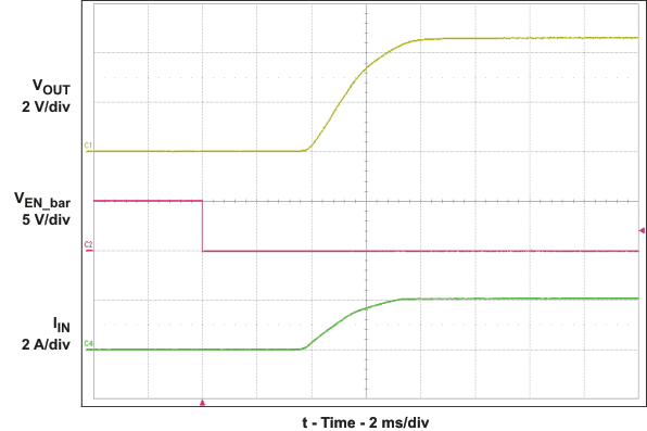 Figure 1. Turnon Delay and Rise Time
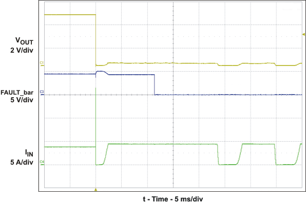
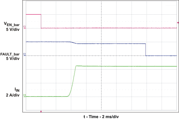 Figure 3. Device Enabled into Short-Circuit
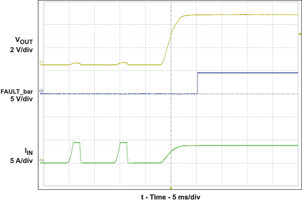 Figure 5. Short-Circuit to Full-Load Recovery Response
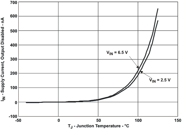 Figure 7. Supply Current, Output Disabled
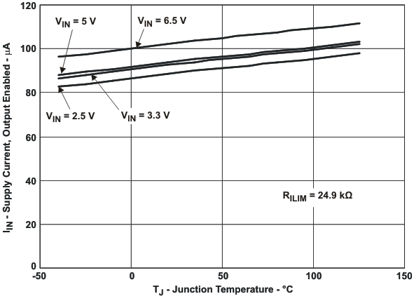
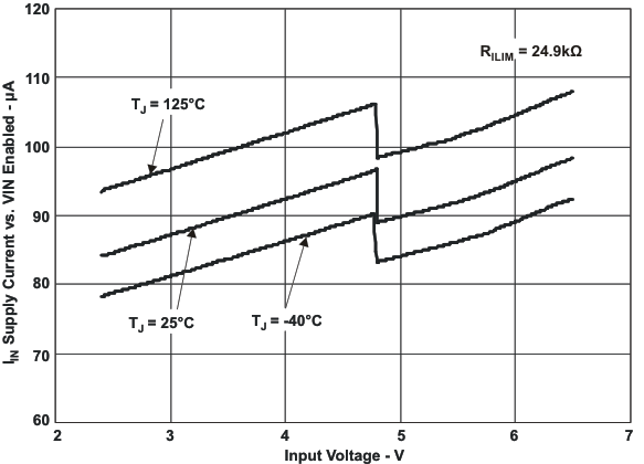 Figure 9. Supply Current, Output Enabled
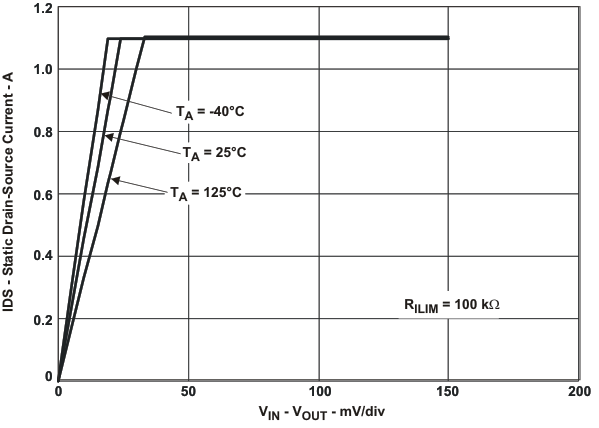
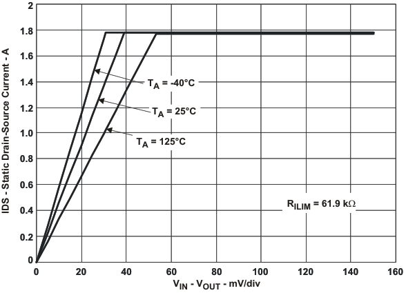
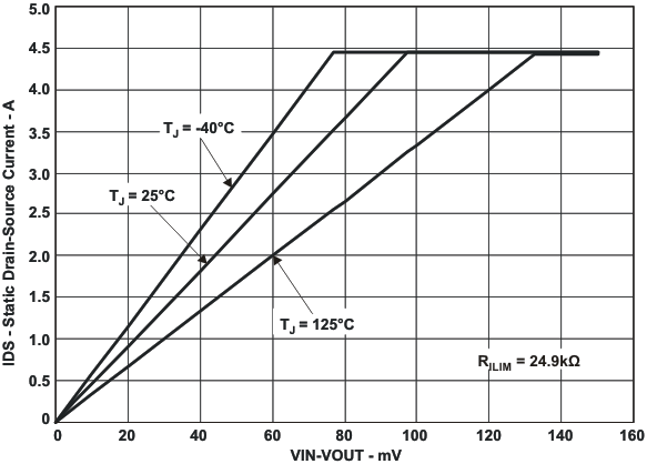 Figure 13. Switch Current vs Drain-Source Voltage Across Switch
