ZHCSF84B April 2016 – June 2017 TPS25740 , TPS25740A
PRODUCTION DATA.
- 1 特性
- 2 应用
- 3 说明
- 4 修订历史记录
- 5 Device Comparison Table
- 6 Pin Configuration and Functions
- 7 Specifications
-
8 Detailed Description
- 8.1 Overview
- 8.2 Functional Block Diagram
- 8.3
Feature Description
- 8.3.1 USB Type-C CC Logic (CC1, CC2)
- 8.3.2 USB PD BMC Transmission (CC1, CC2, VTX)
- 8.3.3 USB PD BMC Reception (CC1, CC2)
- 8.3.4 Discharging (DSCG, VPWR)
- 8.3.5 Configuring Voltage Capabilities (HIPWR, EN9V, EN12V)
- 8.3.6 Configuring Power Capabilities (PSEL, PCTRL, HIPWR)
- 8.3.7 Gate Driver (GDNG, GDNS)
- 8.3.8 Fault Monitoring and Protection
- 8.3.9 Voltage Control (CTL1, CTL2)
- 8.3.10 Sink Attachment Indicator (UFP, DVDD)
- 8.3.11 Power Supplies (VAUX, VDD, VPWR, DVDD)
- 8.3.12 Grounds (AGND, GND)
- 8.3.13 Output Power Supply (DVDD)
- 8.4 Device Functional Modes
-
9 Application and Implementation
- 9.1
Application Information
- 9.1.1 System-Level ESD Protection
- 9.1.2 Use of GD Internal Clamp
- 9.1.3 Resistor Divider on GD for Programmable Start Up
- 9.1.4 Selection of the CTL1 and CTL2 Resistors (R(FBL1) and R(FBL2))
- 9.1.5 Voltage Transition Requirements
- 9.1.6 VBUS Slew Control using GDNG C(SLEW)
- 9.1.7 Tuning OCP Using RF and CF
- 9.2 Typical Application , A/C Power Source (Wall Adapter)
- 9.3 System Examples
- 9.1
Application Information
- 10Power Supply Recommendations
- 11Layout
- 12器件和文档支持
- 13机械、封装和可订购信息
11 Layout
11.1 Port Current Kelvin Sensing
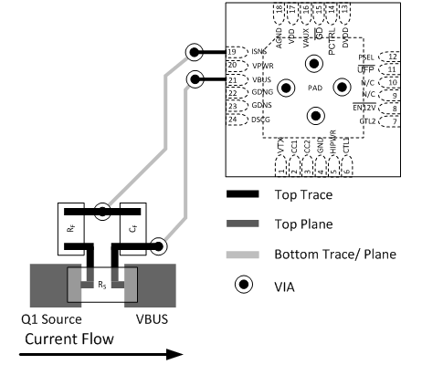
Figure 67 provides a routing example for accurate current sensing for the overcurrent protection feature. The sense amplifier measurement occurs between the ISNS and VBUS pins of the device. Improper connection of these pins can result in poor OCP performance.
 Figure 67. Kelvin Sense Layout Example
11.2 Layout Guidelines
11.2.1 Power Pin Bypass Capacitors
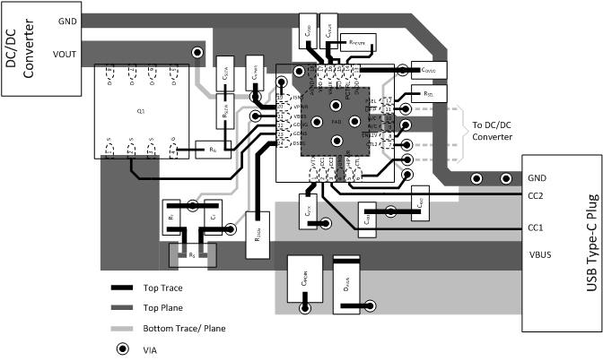
- C(VPWR): Place close to pin 20 (VPWR) and connect with low inductance traces and vias according to Figure 68.
- C(VDD): Place close to pin 17 (VDD) and connect with low inductance traces and vias according to Figure 68.
- C(DVDD): Place close to pin 13 (DVDD) and connect with low inductance traces and vias according to Figure 68.
- C(VAUX): Place close to pin 16 (VAUX) and connect with low inductance traces and vias according to Figure 68.
- C(VTX): Place close to pin 1 (VTX) and connect with low inductance traces and vias according to Figure 68.
11.2.2 Supporting Components
- C(RX): Place C(RX1) and C(RX2) in line with the CC1 and CC2 traces as shown in Figure 23. These should be placed within one inch from the Type C connector. Minimize stubs and tees from on the trace routes.
- Q1: Place Q1 in a manner such that power flows uninterrupted from Q1 drain to the Type C connector VBUS connections. Provide adequate copper plane from Q1 drain and source to the interconnecting circuits.
- RS: Place RS as shown in Figure 68 to facilitate uninterrupted power flow to the Type C connector. Orient RS for optimal Kelvin sense connection/routing back to the TPS25740 or TPS25740A. In high current applications where the power dissipation is over 250 mW, provide an adequate copper feed to the pads of RS.
- RG: Place RG near Q1 as shown in Figure 68. Minimize stray leakage paths as the GDNG sourcing current could be affected.
- R(SLEW)/C(SLEW): Place R(SLEW) and C(SLEW) near RG as shown in Figure 68.
- R(DSCG): Place on top of the VBUS copper route and connect to the DSCG pin with a 15 mil trace.
- RF/CF: When required, place RF and CF as shown in Figure 68 to facilitate the Kelvin sense connection back to the device.
- C(VBUS)/D(VBUS): Place C(VBUS) and D(VBUS) within one inch of the Type C connector and connect them to VBUS and GND using adequate copper shapes.
- R(SEL)/R(PCTRL): Place R(SEL) and R(PCTRL) near the device.
