ZHCSF84B April 2016 – June 2017 TPS25740 , TPS25740A
PRODUCTION DATA.
- 1 特性
- 2 应用
- 3 说明
- 4 修订历史记录
- 5 Device Comparison Table
- 6 Pin Configuration and Functions
- 7 Specifications
-
8 Detailed Description
- 8.1 Overview
- 8.2 Functional Block Diagram
- 8.3
Feature Description
- 8.3.1 USB Type-C CC Logic (CC1, CC2)
- 8.3.2 USB PD BMC Transmission (CC1, CC2, VTX)
- 8.3.3 USB PD BMC Reception (CC1, CC2)
- 8.3.4 Discharging (DSCG, VPWR)
- 8.3.5 Configuring Voltage Capabilities (HIPWR, EN9V, EN12V)
- 8.3.6 Configuring Power Capabilities (PSEL, PCTRL, HIPWR)
- 8.3.7 Gate Driver (GDNG, GDNS)
- 8.3.8 Fault Monitoring and Protection
- 8.3.9 Voltage Control (CTL1, CTL2)
- 8.3.10 Sink Attachment Indicator (UFP, DVDD)
- 8.3.11 Power Supplies (VAUX, VDD, VPWR, DVDD)
- 8.3.12 Grounds (AGND, GND)
- 8.3.13 Output Power Supply (DVDD)
- 8.4 Device Functional Modes
-
9 Application and Implementation
- 9.1
Application Information
- 9.1.1 System-Level ESD Protection
- 9.1.2 Use of GD Internal Clamp
- 9.1.3 Resistor Divider on GD for Programmable Start Up
- 9.1.4 Selection of the CTL1 and CTL2 Resistors (R(FBL1) and R(FBL2))
- 9.1.5 Voltage Transition Requirements
- 9.1.6 VBUS Slew Control using GDNG C(SLEW)
- 9.1.7 Tuning OCP Using RF and CF
- 9.2 Typical Application , A/C Power Source (Wall Adapter)
- 9.3 System Examples
- 9.1
Application Information
- 10Power Supply Recommendations
- 11Layout
- 12器件和文档支持
- 13机械、封装和可订购信息
7 Specifications
7.1 Absolute Maximum Ratings
over operating free-air temperature range (unless otherwise noted)(1)| MIN | MAX | UNIT | ||
|---|---|---|---|---|
| Pin Voltage (sustained) | VDD , EN12V, EN9V, CTL1, CTL2, UFP, PCTRL, CC1, CC2 | –0.3 | 6 | V |
| VTX(2) | –0.3 | 2.1 | V | |
| VAUX(2) | –0.3 | 4.5 | V | |
| GD (3) | –0.3 | 7 | V | |
| HIPWR, PSEL, DVDD (2) | –0.3 | 2.1 | V | |
| GDNG(2) | –0.5 | 40 | V | |
| VBUS,VPWR, ISNS, DSCG, GDNS | –0.5 | 30 | V | |
| Pin Voltage (transient for 1ms) | VBUS,VPWR, ISNS, DSCG, GDNS | –1.5 | 30 | V |
| Pin-to-pin voltage | V(GDNG) – V(GDNS) | –0.3 | 20 | V |
| AGND to GND | –0.3 | 0.3 | V | |
| ISNS to VBUS | –0.3 | 0.3 | V | |
| Sinking current (average) | CTL1, CTL2, UFP | 8 | mA | |
| GD | 100 | µA | ||
| DSCG | 10 | mA | ||
| Sinking current (transient, 50 ms pulse 0.25% duty cycle) | DSCG | 375 | mA | |
| Current sourcing | VTX | Internally limited | mA | |
| CC1, CC2 | Internally limited | mA | ||
| VAUX | 0 | 25 | µA | |
| Operating junction temperature range, TJ | –40 | 125 | °C | |
| Storage temperature, Tstg | –65 | 150 | °C | |
(1) Stresses beyond those listed under Absolute Maximum Ratings may cause permanent damage to the device. These are stress ratings only, which do not imply functional operation of the device at these or any other conditions beyond those indicated under Recommended Operating Conditions. Exposure to absolute-maximum-rated conditions for extended periods may affect device reliability.
(2) Do not apply voltage to these pins.
(3) Voltage allowed to rise above Absolute Maximum provided current is limited.
7.2 ESD Ratings(3)
| VALUE | UNIT | |||
|---|---|---|---|---|
| V(ESD) | Electrostatic discharge | Human-body model (HBM), per ANSI/ESDA/JEDEC JS-001(1) | ±2500 | V |
| Charged-device model (CDM), per JEDEC specification JESD22-C101(2) | ±1000 | |||
| IEC (4) 61000-4-2 contact discharge, CC1, CC2 | ±8000 | |||
| IEC (4) 61000-4-2 air-gap discharge, CC1, CC2 | ±15000 | |||
(1) JEDEC document JEP155 states that 500-V HBM allows safe manufacturing with a standard ESD control process.
(2) JEDEC document JEP157 states that 250-V CDM allows safe manufacturing with a standard ESD control process.
(3) This integrated circuit can be damaged by ESD. Texas Instruments recommends that all integrated circuits be handled with appropriate precautions. Failure to observe proper handling and installation procedures can cause damage.
(4) These results were passing limits that were obtained on an application-level test board. Individual results may vary based on implementation. Surges per IEC61000-4-2, 1999 applied between CC1/CC2 and ground of TPS25740EVM-741 and TPS25740AEVM-741
7.3 Recommended Operating Conditions
over operating free-air temperature range (unless otherwise noted)| MIN | NOM | MAX | UNIT | |||
|---|---|---|---|---|---|---|
| VIN | Supply Voltage | VDD | 0 | 5.5 | V | |
| VPWR | 4.65 | 25 | V | |||
| VI | Applied Voltage | EN12V, EN9V, PCTRL, CC1, CC2, CTL1, CTL2 | 0 | 5.5 | V | |
| GD | 0 | 6.5 | V | |||
| DSCG, GDNS, VBUS | 0 | 25 | V | |||
| HIPWR, PSEL | 0 | DVDD | V | |||
| VI | Pin-to-pin voltage | ISNS - VBUS | –0.1 | 0.1 | V | |
| VIH | High-Level Input Voltage | EN12V, EN9V | 1.4 | V | ||
| PCTRL | 2 | V | ||||
| GD | 2 | V | ||||
| VIL | Low-Level Input Voltage | EN12V, EN9V | 0.5 | V | ||
| PCTRL | 1.6 | V | ||||
| GD | 1.6 | V | ||||
| IS | Sinking Current | CTL1, CTL2, UFP | 5 | mA | ||
| GD | 80 | µA | ||||
| DSCG, transient sinking current 50 ms pulse, 0.25% duty cycle | 350 | mA | ||||
| DSCG, average | 5 | mA | ||||
| CS | Shunt capacitance | CC1, CC2 (C(RX)) | 200 | 560 | 600 | pF |
| VBUS (C(PDIN)) | 10 | µF | ||||
| DVDD (C(DVDD)) | 0.198 | 0.22 | 0.242 | µF | ||
| VAUX (C(VAUX)) | 0.09 | 0.1 | 0.11 | µF | ||
| VTX (C(VTX)) | 0.09 | 0.10 | 0.11 | µF | ||
| VDD (C(VDD)) | 0.09 | µF | ||||
| RS | Sense resistance | Configured for 3 A | 5 | 6.4 | mΩ | |
| Configured for 5 A | 5 | 5.8 | mΩ | |||
| R(PUD) | Pull up/down resistance | HIPWR, PSEL (direct to GND or direct to DVDD) | 0 | 1 | kΩ | |
| HIPWR, PSEL (R(SEL) ) | 80 | 100 | 120 | kΩ | ||
| R(DSCG) | Series resistance | Maximum VBUS voltage of 25 V | 80 | Ω | ||
| Maximum VBUS voltage of 15 V | 43 | Ω | ||||
| Maximum VBUS voltage of 6 V | 20 | Ω | ||||
| TJ | Operating junction temperature | -40 | 125 | °C | ||
7.4 Thermal Information
| THERMAL METRIC(1) | TPS25740 TPS25740A |
UNIT | |
|---|---|---|---|
| RGE (VQFN) | |||
| 24 PINS | |||
| RθJA | Junction-to-ambient thermal resistance | 33 | °C/W |
| RθJC(top) | Junction-to-case (top) thermal resistance | 32.6 | °C/W |
| RθJB | Junction-to-board thermal resistance | 10 | °C/W |
| ψJT | Junction-to-top characterization parameter | 0.4 | °C/W |
| ψJB | Junction-to-board characterization parameter | 10 | °C/W |
| RθJC(bot) | Junction-to-case (bottom) thermal resistance | 2.6 | °C/W |
(1) For more information about traditional and new thermal metrics, see the Semiconductor and IC Package Thermal Metrics application report.
7.5 Electrical Characteristics
Unless otherwise stated in a specific test condition the following conditions apply: –40°C ≤ TJ ≤ 125°C; 3 ≤ VDD ≤ 5.5 V, 4.65 V ≤ VPWR ≤ 25 V; HIPWR = GND, PSEL = GND, GD = VAUX, PCTRL = VAUX, AGND = GND; VAUX, VTX, bypassed with 0.1 µF, DVDD bypassed with 0.22 µF, EN12V = GND and EN9V = GND; all other pins open (unless otherwise noted)| PARAMETER | TEST CONDITIONS | MIN | TYP | MAX | UNIT | |
|---|---|---|---|---|---|---|
| Voltage Comparator (VBUS) | ||||||
| V(VBUS_RTH) | VBUS Threshold (Rising voltage) | 4.25 | 4.45 | 4.65 | V | |
| V(VBUS_FTH) | VBUS Threshold (Falling voltage) | 3.5 | 3.7 | 3.9 | V | |
| VBUS Threshold (Hysteresis) | 0.75 | V | ||||
| Power Supply (VDD, VPWR) | ||||||
| V(VDD_TH) | VDD UVLO threshold | Rising voltage | 2.8 | 2.91 | 2.97 | V |
| Falling voltage | 2.8 | 2.86 | 2.91 | |||
| Hysteresis, comes into effect once the rising threshold is crossed. | 0.05 | |||||
| V(VPWR_RTH) | VPWR UVLO threshold rising | Rising voltage | 4.2 | 4.45 | 4.65 | V |
| V(VPWR_FTH) | VPWR UVLO threshold falling | Falling voltage | 3.5 | 3.7 | 3.9 | V |
| VPWR UVLO threshold hysteresis | Hysteresis, comes into effect once the rising threshold is crossed. | 0.75 | V | |||
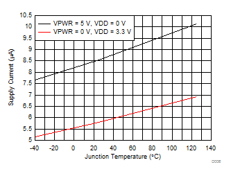
| Supply current drawn from VDD in sleep mode | VPWR = 0 V, VDD = 5 V, CC1 and CC2 pins are open. | 9.2 | 20 | µA | ||
| VPWR = 0 V, VDD = 5 V,CC1 pin open, CC2 pin tied to GND. | 94 | 150 | µA | |||
| Supply current drawn from VPWR in sleep mode | VPWR = 5 V, VDD = 0 V, CC1 and CC2 pins are open. | 8.5 | 15 | µA | ||
| VPWR = 5 V, VDD = 0 V, CC1 pin open, CC2 pin tied to GND. | 90 | 140 | µA | |||
| I(SUPP) | Operating current while sink attached | PD Sourcing active, VBUS = 5 V, VPWR = 5 V, VDD = 3.3 V |
1 | 1.8 | 3 | mA |
| Over/Under Voltage Protection (VBUS) | ||||||
| V(FOVP) | Fast OVP threshold, always enabled | 5 V PD contract | 5.8 | 6.05 | 6.3 | V |
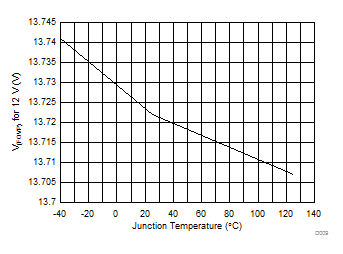
| 12 V PD contract (TPS25740) | 13.2 | 13.75 | 14.3 | V | ||
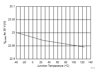
| 20 V PD contract (TPS25740) | 22.1 | 23.05 | 24.0 | V | ||
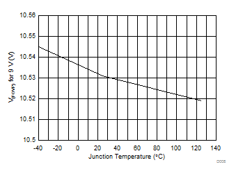
| 9 V PD contract (TPS25740A) | 10.1 | 10.55 | 11.0 | V | ||
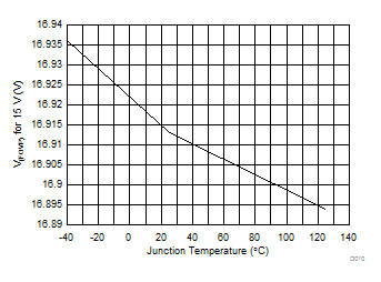
| 15 V PD contract (TPS25740A) | 16.2 | 16.95 | 17.7 | V | ||
| V(SOVP) | Slow OVP threshold, disabled during voltage transitions. (See Figure 1) | 5 V PD contract | 5.5 | 5.65 | 5.8 | V |
| 12 V PD contract (TPS25740) | 13.1 | 13.4 | 13.7 | V | ||
| 20 V PD contract (TPS25740) | 21.5 | 22.0 | 22.5 | V | ||
| 9 V PD contract (TPS25740A) | 10 | 10.2 | 10.4 | V | ||
| 15 V PD contract (TPS25740A) | 16.3 | 16.5 | 17 | V | ||
| V(SUVP) | UVP threshold, disabled during voltage transitions (See Figure 1) | 5 V PD contract | 3.5 | 3.65 | 3.8 | V |
| 12 V PD contract (TPS25740) | 9.2 | 9.45 | 9.7 | V | ||
| 20 V PD contract (TPS25740) | 15.7 | 16.1 | 16.5 | V | ||
| 9 V PD contract (TPS25740A) | 6.8 | 6.95 | 7.1 | V | ||
| 15 V PD contract (TPS25740A) | 11.7 | 11.95 | 12.2 | V | ||
| VAUX | ||||||
| V(VAUX) | Output voltage | 0 ≤ I(VAUX) ≤ I(VAUXEXT) | 2.875 | 3.2 | 4.1 | V |
| VAUX Current limit | 1 | 5 | mA | |||
| I(VAUXEXT) | External load that may be applied to VAUX. | 25 | µA | |||
| DVDD | ||||||
| V(DVDD) | Output voltage | 0 mA ≤ I(DVDD) ≤ 35 mA, CC1 or CC2 pulled to ground via 5.1 kΩ, or both CC1 and CC2 pulled to ground via 1 kΩ | 1.75 | 1.85 | 1.95 | V |
| Load Regulation | Overshoot from V(DVDD), 10-mA minimum, 0.198-µF bypass capacitor |
1.7 | 2 | V | ||
| Current limit | DVDD tied to GND | 40 | 150 | mA | ||
| VTX | ||||||
| Output voltage | Not transmitting or receiving, 0 to 2 mA external load | 1.050 | 1.125 | 1.200 | V | |
| Current Limit | VTX tied to GND | 2.5 | 10 | mA | ||
| Gate Driver Disable (GD) | ||||||
| V(GD_TH) | Input enable threshold voltage | Rising voltage | 1.64 | 1.725 | 1.81 | V |
| Hysteresis | 0.15 | V | ||||
| V(GDC) | Internal clamp voltage | I(GD) = 80 µA | 6.5 | 7 | 8.5 | V |
| R(GD) | Internal pulldown resistance | From 0 V to 6 V | 3 | 6 | 9.5 | MΩ |
| Discharge (DSCG) (1)(2) | ||||||
| V(DSCGT) | ON state (linear) | I(DSCG) = 100 mA | 0.15 | 0.42 | 1 | V |
| I(DSCGT) | ON state (saturation) | V(DSCG) = 4 V, pulsed mode operation | 220 | 553 | 1300 | mA |
| R(DSCGB) | Discharge bleeder | While CC1 is pulled down by 5.1 kΩ and CC2 is open, V(DSCG) = 25 V | 6.6 | 8.2 | 10 | kΩ |
| Leakage current | 0 V ≤ V(DSCG) ≤ 25 V | 2 | µA | |||
| N-ch MOSFET Gate Driver (GDNG,GDNS) | ||||||
| I(GDNON) | Sourcing current | 0 V ≤ V(GDNS) ≤ 25 V, 0 V ≤ V(GDNG) – V(GDNS) ≤ 6 V |
13.2 | 20 | 30 | µA |
| V(GDNON) | Sourcing voltage while enabled (V(GDNG)– V(GDNS)) |
0 V ≤ V(GDNS) ≤ 25 V, I(GDNON) ≤ 4 µA, VPWR = 0 V | 7 | 12 | V | |
| 0 V ≤ V(GDNS) ≤ 25 V, I(GDNON) ≤ 4 µA, VDD = 0 V | 8.5 | 12 | V | |||
| R(GDNGOFF) | Sinking strength while disabled | V(GDNG) – V(GDNS)= 0.5 V, 0 ≤ V(GDNS) ≤ 25 V |
150 | 300 | Ω | |
| Sinking strength UVLO (safety) | VDD = 1.4 V, V(GDNG) = 1 V, V(GDNS) = 0 V, VPWR = 0 V |
145 | µA | |||
| VPWR = 1.4 V, V(GDNG) = 1 V, V(GDNS) = 0 V, VDD = 0 V |
145 | µA | ||||
| Off-state leakage | V(GDNS) = 25 V, V(GDNG) open | 7 | µA | |||
| Power Control Input (PCTRL) | ||||||
| V(PCTRL_TH) | Threshold voltage(3) | Voltage rising | 1.65 | 1.75 | 1.85 | V |
| Hysteresis | 100 | mV | ||||
| Input resistance | 0 V ≤ V(PCTRL) ≤ V(VAUX) | 1.5 | 2.9 | 6 | MΩ | |
| Voltage Select (HIPWR), Power Select (PSEL)(4) | ||||||
| Leakage current | 0 V ≤ V(HIPWR) ≤ V(DVDD), 0 V ≤ V(PSEL) ≤ V(DVDD) |
–1 | 1 | µA | ||
| Port Status and Voltage Control (CTL1, CTL2, UFP)(5) | ||||||
| VOL | Output low voltage | IOL = 4 mA sinking | 0.4 | V | ||
| Leakage Current (6) | In Hi-Z state, 0 ≤ V(CTLx) ≤ 5.5 V or 0 ≤ VUFP ≤ 5.5V |
–0.5 | 0.5 | µA | ||
| Enable 9 V, 12 V Capability (EN9V, EN12V) | ||||||
| Input low threshold voltage | 0.585 | V | ||||
| Input high threshold voltage | 1.225 | V | ||||
| Input hysteresis | 0.25 | V | ||||
| Transmitter Specifications (CC1, CC2) | ||||||
| RTX | Output resistance (zDriver from USB PD in 文档支持) | During transmission | 33 | 45 | 75 | Ω |
| V(TXHI) | Transmit high voltage | External Loading per Figure 25 | 1.05 | 1.125 | 1.2 | V |
| V(TXLO) | Transmit low voltage | External Loading per Figure 25 | –75 | 75 | mV | |
| Receiver Specifications (CC1, CC2) | ||||||
| V(RXHI) | Receive threshold (rising) | 800 | 840 | 885 | mV | |
| V(RXLO) | Receive threshold (falling) | 485 | 525 | 570 | mV | |
| Receive threshold (Hysteresis) | 315 | mV | ||||
| V(INT) | Amplitude of interference that can be tolerated | Interference is 600 kHz square wave, rising 0 to 100 mV. | 100 | mV | ||
| Interference is 1 MHz sine wave | 1 | VPP | ||||
| DFP Specifications (CC1, CC2) | ||||||
| V(DSTD) | Detach threshold when cable is detached. | In standard DFP mode(7), voltage rising | 1.52 | 1.585 | 1.65 | V |
| Hysteresis | 0.02 | V | ||||
| V(D1.5) | In 1.5 A DFP mode(8), voltage rising | 1.52 | 1.585 | 1.65 | V | |
| Hysteresis | 0.02 | V | ||||
| V(D3.0) | In 3 A DFP mode(9), voltage rising | 2.50 | 2.625 | 2.75 | V | |
| Hysteresis | 0.05 | V | ||||
| V(OCN) | Unloaded output voltage on CC pin | normal mode | 2.7 | 4.35 | V | |
| V(OCDS) | VPWR = 0 V (in UVLO) or in sleep mode | 1.8 | 5.5 | V | ||
| I(RPSTD) | Loaded output current while connected through CCx | In standard DFP mode1, CCy open, 0 V ≤ VCCx ≤ 1.5 V (vRd) |
64 | 80 | 96 | µA |
| I(RP1.5) | In 1.5 A DFP mode 2, CCy open, 0 V ≤ VCCx ≤ 1.5 V (vRd) |
166 | 180 | 194 | µA | |
| I(RP3.0) | In 3 A DFP mode 3, CCy open, 0 V ≤ VCCx ≤ 1.5 V (vRd) |
304 | 330 | 356 | µA | |
| V(RDSTD) | Ra, Rd detection threshold (falling) | In standard DFP mode1, 0 V ≤ VCCx ≤ 1.5 V (vRd) |
0.15 | 0.19 | 0.23 | V |
| Hysteresis | 0.02 | V | ||||
| V(RD1.5) | In 1.5 A DFP mode2, CCy open 0 V ≤ VCCx ≤ 1.5 V (vRd) |
0.35 | 0.39 | 0.43 | V | |
| Hysteresis | 0.02 | V | ||||
| V(RD3.0) | In 3 A DFP mode3, CCy open 0 V ≤ VCCx ≤ 1.5 V (vRd) |
0.75 | 0.79 | 0.83 | V | |
| Hysteresis | 0.02 | V | ||||
| V(WAKE) | Wake threshold (rising and falling), exit from sleep mode | VPWR = 4.65 V , 0 V ≤ VDD ≤ 3 V | 1.6 | 3.0 | V | |
| I(DSDFP) | Output current on CCx in sleep mode to detect Ra removal. | CCx = 0V, CCy floating | 40 | 73 | 105 | µA |
| OverCurrent Protection (ISNS, VBUS) | ||||||
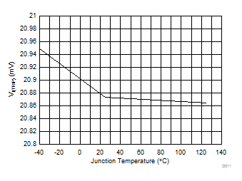
| VI(TRIP) | Current trip shunt voltage | Specified as V(ISNS)-V(VBUS). 3.5 V(10) ≤ VBUS ≤ 25 V |
||||
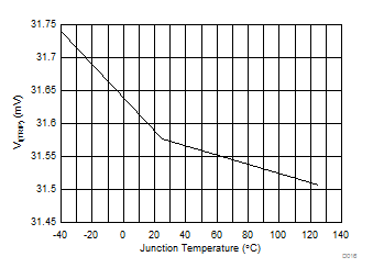
| HIPWR: 5 A not enabled | 19.2 | 22.6 | mV | |||
| HIPWR = DVDD (5 A enabled) | 29 | 34 | mV | |||
| OTSD | ||||||
| TJ1 | Die Temperature (Analog)(11) | TJ ↑ | 125 | 135 | 145 | °C |
| Hysteresis | 10 | |||||
| TJ2 | Die Temperature (Analog) (12) | TJ ↑ | 140 | 150 | 163 | °C |
| Hysteresis | 10 | |||||
(1) If TJ1 is perceived to have been exceeded an OTSD occurs and the discharge FET is disabled.
(2) The discharge pull-down is not active in the sleep mode.
(3) When voltage on the PCTRL pin is less than V(PCTRL_TH), the amount of power advertised is reduced by half.
(4) Leaving HIPWR or PSEL open is an undetermined state and leads to unpredictable behavior.
(5) These pins are high-z during a UVLO, reset, or in Sleep condition.
(6) The pins were designed for less leakage, but testing only verifies that the leakage does not exceed 0.5 µA.
(7) Standard DFP mode is active after a USB Type-C sink, debug accessory, or audio accessory is attached until the first USB PD message is transmitted (after GDNG has been enabled).
(8) 1.5 A DFP mode is active after a USB PD message is received.
(9) 3 A DFP mode is active after GDNG has been enabled until a USB PD message is received.
(10) Common mode minimum aligns to VBUS UVLO. VBUS must be above its UVLO for the OCP function to be active.
(11) When TJ1 trips a hard reset is transmitted and discharge is disabled, but the bleed discharge is not disabled.
(12) TJ2 trips only when some external heat source drives the temperature up. When it trips the DVDD, and VAUX power outputs are turned off.
7.6 Timing Requirements
Unless otherwise stated in a specific test condition the following conditions apply: –40°C ≤ TJ ≤ 125°C; 3 ≤ VDD ≤ 5.5 V, 4.65 V ≤ VPWR ≤ 25 V; HIPWR = GND, PSEL = GND, GD = VAUX, PCTRL = VAUX, AGND = GND; VAUX, VTX, bypassed with 0.1 µF, DVDD bypassed with 0.22 µF, EN12V = GND and EN9V = GND; all other pins open (unless otherwise noted)| MIN | NOM | MAX | UNIT | |||
|---|---|---|---|---|---|---|
| tFOVPDG | Deglitch for fast over-voltage protection | 5 | µs | |||
| tOCP | Deglitch Filter for over-current protection | 15 | µs | |||
| Time power is applied until CC1 and CC2 pull-ups are applied. | V(VPWR) > V(VPWR_TH) OR V(VDD) > V(VDD_TH) |
2.5 | 4 | ms | ||
| tCC | Falling/Rising voltage deglitch time for detection on CC1 and CC2 | 120 | µs | |||
| Transmitter Specifications (CC1, CC2) | ||||||
| tUI | Bit unit Interval | 3.05 | 3.3 | 3.70 | µs | |
| Rise/fall time, tFall and tRise (refer to USB PD in 文档支持) | External Loading per Figure 25 | 300 | 600 | ns | ||
7.7 Switching Characteristics
Unless otherwise stated in a specific test condition the following conditions apply: –40°C ≤ TJ ≤ 125°C; 3 ≤ VDD ≤ 5.5 V, 4.65 V ≤ VPWR ≤ 25 V; HIPWR = GND, PSEL = GND, GD = VAUX, PCTRL = VAUX, AGND = GND; VAUX, VTX, bypassed with 0.1 µF, DVDD bypassed with 0.22 µF, EN12V = GND and EN9V = GND; all other pins open (unless otherwise noted)| PARAMETER | TEST CONDITIONS | MIN | TYP | MAX | UNIT | |
|---|---|---|---|---|---|---|
| tVP | Delay from enabling external NFET until under-voltage and OCP protection are enabled | VBUS = GND | 190 | ms | ||
| tSTL | Source settling time, time from CTL1 and CTL2 being changed until a PS_RDY USB PD message is transmitted to inform the sink is may draw full current. (refer to USB PD in 文档支持) | 260 | ms | |||
| tSR | Time that GDNG is disabled after a hard reset. This is tSrcRecover. (refer to USB PD in 文档支持) | TJ > TJ1 | 765 | ms | ||
| tHR | Time after hard reset is transmitted until GDNG is disabled. This is tPSHardReset. (refer to USB PD in 文档支持) | 30 | ms | |||
| tCCDeb | Time until UFP is pulled low after sink attachment, this is the USB Type-C required debounce time for attachment detection called tCCDebounce. (refer to USB Type-C in 文档支持) | 185 | ms | |||
| tST | Delay after sink request is accepted until CTL1 and/or CTL2 is changed. This is called tSnkTransition. (refer to USB PD in 文档支持) | 30 | ms | |||
| tFLT | The time in between hard reset transmissions in the presence of a persistent supply fault. | GD = GND or VPWR=GND, sink attached | 1395 | ms | ||
| tSH | The time in between retries (hard reset transmissions) in the presence of a persistent VBUS short. | VBUS = GND, sink attached | 985 | ms | ||
| tON | The time from UFP being pulled low until a hard reset is transmitted. Designed to be greater than tSrcTurnOn. (refer to USB PD in 文档支持) | GD = 0 V or VPWR = 0 V | 600 | ms | ||
| Retry interval if USB PD sink stops communicating without being removed or if sink does not communicate after a fault condition. Time GDNG remains enabled before a hard reset is transmitted. This is the tNoResponse time. (refer to USB PD in 文档支持) | Sink attached | 4.8 | s | |||
| tDVDD | Delay before DVDD is driven high | After sink attached | 5 | ms | ||
| tGDoff | Turnoff delay, time until V(GDNG) is below 10% of its initial value after the GD pin is low. | VGD: 5 V → 0 V in < 0.5 µs. | 5 | µs | ||
| tFOVP | Response time when VBUS exceeds the fast-OVP threshold | VBUS ↑ to GDNG OFF (V(GDNG) below 10% its initial value) |
30 | µs | ||
| OCP large signal response time | 5 A enabled, V(ISNS) -V(VBUS): 0 V → 42 mV measured to GDNG transition start. | 30 | µs | |||
| Time until discharge is stopped after TJ1 is exceeded. | 0 V ≤ V(DSCG) ≤ 25 V | 10 | µs | |||
| Digital output fall time | V(PULLUP) = 1.8 V, CL = 10 pF, R(PULLUP) = 10 kΩ, V(CTLx) or V(UFP) : 70% VPULLUP → 30% VPULLUP |
20 | 300 | ps | ||
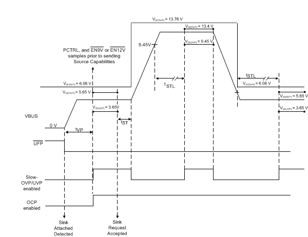 Figure 1. Timing Illustration for tVP, tST and tSTL, After Sink Attachment negotiation to 12 V then back to 5 V. V(SOVP) and V(SUVP) are Disabled Around Voltage Transitions.
 Figure 2. Timing Illustration for tHR and tSR, After Sink Attachment with persistent TJ > TJ1
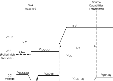 Figure 3. Timing Illustration for tCcDeb and tVP, Under Persistent Fault Condition
 Figure 4. Timing Illustration for tSH and tVP, with VBUS Shorted to Ground
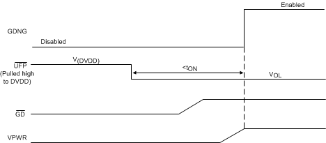 Figure 5. Timing Illustration for tON
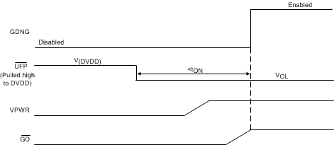 Figure 6. Timing Illustration for tON
7.8 Typical Characteristics
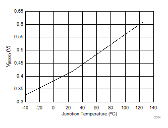
| I(DSCG) = 100 mA |
A.
Figure 15. VI(TRIP) When V(VPWR) > 4.65 V
| 5 A enabled |
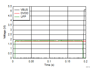
| Sink attached at time 0 | ||
| UFP pulled up to DVDD | ||
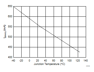
| V(DSCG) = 4 V | Pulsed Testing |
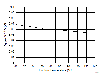
| 3 A enabled |
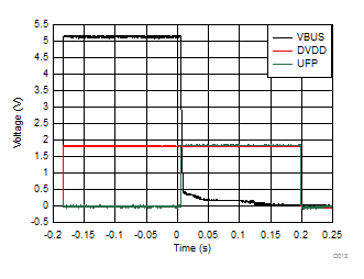
| Sink detached at time 0s | ||
| Sleep mode entered at time 0.19s. | ||
| UFP pulled up to DVDD |