ZHCSGV1C June 2017 – March 2018 TPS25740B
PRODUCTION DATA.
- 1 特性
- 2 应用
- 3 说明
- 4 修订历史记录
- 5 Device Comparison Table
- 6 Pin Configuration and Functions
- 7 Specifications
-
8 Detailed Description
- 8.1 Overview
- 8.2 Functional Block Diagram
- 8.3
Feature Description
- 8.3.1 ENSRC
- 8.3.2 USB Type-C CC Logic (CC1, CC2)
- 8.3.3 USB PD BMC Transmission (CC1, CC2, VTX)
- 8.3.4 USB PD BMC Reception (CC1, CC2)
- 8.3.5 Discharging (DSCG, VPWR)
- 8.3.6 Configuring Voltage Capabilities (HIPWR)
- 8.3.7 Configuring Power Capabilities (PSEL, PCTRL, HIPWR)
- 8.3.8 Gate Driver (GDNG, GDNS)
- 8.3.9 Fault Monitoring and Protection
- 8.3.10 Voltage Control (CTL1, CTL2,CTL3)
- 8.3.11 Sink Attachment Indicator (DVDD)
- 8.3.12 Power Supplies (VAUX, VDD, VPWR, DVDD)
- 8.3.13 Grounds (AGND, GND)
- 8.3.14 Output Power Supply (DVDD)
- 8.4 Device Functional Modes
-
9 Application and Implementation
- 9.1
Application Information
- 9.1.1 System-Level ESD Protection
- 9.1.2 Using ENSRC to Enable the Power Supply upon Sink Attachment
- 9.1.3 Use of GD Internal Clamp
- 9.1.4 Resistor Divider on GD for Programmable Start Up
- 9.1.5 Selection of the CTL1, CTL2, and CTL3 Resistors (R(FBL1), R(FBL2), and R(FBL3))
- 9.1.6 Voltage Transition Requirements
- 9.1.7 VBUS Slew Control using GDNG C(SLEW)
- 9.1.8 Tuning OCP using RF and CF
- 9.2 Typical Applications
- 9.3 System Examples
- 9.1
Application Information
- 10Power Supply Recommendations
- 11Layout
- 12器件和文档支持
- 13机械、封装和可订购信息
8.1 Overview
The TPS25740B and supporting circuits perform the functions required to implement a USB Power Delivery (PD) 2.0 as a provider-only and a USB Type-C revision 1.2 source. It uses its CC pins to detect the attachment of a sinking device or upward facing port (UFP) and to determine which of CC1 or CC2 is connected to the CC wire of the cable. It then communicates over the CC wire in the cable bundle using USB PD to offer a set of voltages and currents. USB PD is a technology that utilizes the ubiquitous USB communications and hardware infrastructure to extend the amount of power available to devices from the 7.5 W range for USB BC1.2 to as high as 100 W in a dock. It is a compatible overlay to USB 2.0 and USB 3.0, coexisting with the existing 5 V powered universe of devices by use of adapter cables. Some basic characteristics of this technology relevant to the device include:
- Increased power achieved by providing higher current and/or higher voltage.
- New 3 A cable and 5 A connector to support greater than the traditional 1.5 A.
- Cables have controlled voltage drop
- Voltages greater than 5 V are negotiated between PD partners.
- Standard 5 V is always the default source voltage.
- Voltage and current provisions are negotiated between PD partners.
- PD partners negotiate over the CC line to avoid conflict with existing signaling (that is, D+, D-)
- Layered communication protocol defined including PHY, Protocol Layer, Policy Engine, and Device Policy Manager all implemented within the device.
- The Type-C connector standard implements pre-powerup signaling to determine:
- Connector orientation
- Source 5-V capability
- Detect through connection of a UFP (upward facing port) to a DFP (downward facing port).
- Detection of when the connected UFP is disconnected. VBUS is unpowered until a through-connection is present
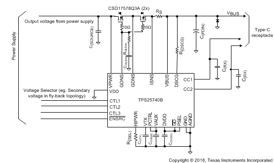
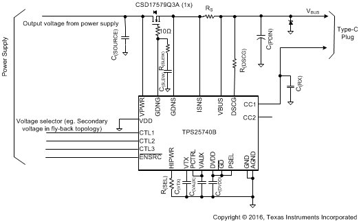
Figure 21 and Figure 22 show a typical configuration for the device.
 Figure 21. Schematic 1
  Figure 22. Schematic 2