ZHCSGV1C June 2017 – March 2018 TPS25740B
PRODUCTION DATA.
- 1 特性
- 2 应用
- 3 说明
- 4 修订历史记录
- 5 Device Comparison Table
- 6 Pin Configuration and Functions
- 7 Specifications
-
8 Detailed Description
- 8.1 Overview
- 8.2 Functional Block Diagram
- 8.3
Feature Description
- 8.3.1 ENSRC
- 8.3.2 USB Type-C CC Logic (CC1, CC2)
- 8.3.3 USB PD BMC Transmission (CC1, CC2, VTX)
- 8.3.4 USB PD BMC Reception (CC1, CC2)
- 8.3.5 Discharging (DSCG, VPWR)
- 8.3.6 Configuring Voltage Capabilities (HIPWR)
- 8.3.7 Configuring Power Capabilities (PSEL, PCTRL, HIPWR)
- 8.3.8 Gate Driver (GDNG, GDNS)
- 8.3.9 Fault Monitoring and Protection
- 8.3.10 Voltage Control (CTL1, CTL2,CTL3)
- 8.3.11 Sink Attachment Indicator (DVDD)
- 8.3.12 Power Supplies (VAUX, VDD, VPWR, DVDD)
- 8.3.13 Grounds (AGND, GND)
- 8.3.14 Output Power Supply (DVDD)
- 8.4 Device Functional Modes
-
9 Application and Implementation
- 9.1
Application Information
- 9.1.1 System-Level ESD Protection
- 9.1.2 Using ENSRC to Enable the Power Supply upon Sink Attachment
- 9.1.3 Use of GD Internal Clamp
- 9.1.4 Resistor Divider on GD for Programmable Start Up
- 9.1.5 Selection of the CTL1, CTL2, and CTL3 Resistors (R(FBL1), R(FBL2), and R(FBL3))
- 9.1.6 Voltage Transition Requirements
- 9.1.7 VBUS Slew Control using GDNG C(SLEW)
- 9.1.8 Tuning OCP using RF and CF
- 9.2 Typical Applications
- 9.3 System Examples
- 9.1
Application Information
- 10Power Supply Recommendations
- 11Layout
- 12器件和文档支持
- 13机械、封装和可订购信息
9.1.4 Resistor Divider on GD for Programmable Start Up
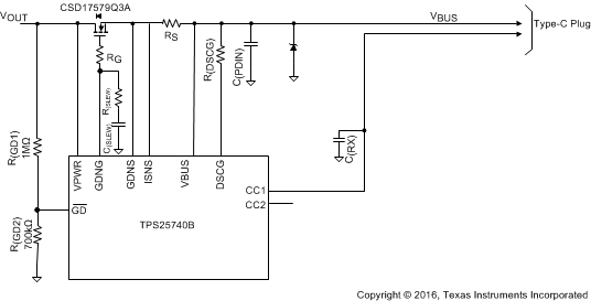
Figure 42 shows an alternative usage of the GD pin can help protect against shorts on the VBUS pin in the receptacle. A resistor divider is used to minimize the time it takes the GD pin to be pulled low. Consider the situation where the VBUS pin is shorted at startup. At some point, the device closes the NFET switch to supply 5 V to VBUS. At that point, the short pulls down on the voltage seen at the VPWR pin. With the resistor values shown in Figure 42, once the voltage at the VPWR pin reaches 3.95 V the voltage at the GD pin is specified to be below V(GD_TH) min. Without the 700-kΩ resistor, the voltage at the VPWR pin would have to reach V(GD_TH) min which takes longer. This comes at the expense of increased leakage current.
 Figure 42. Programmable GD Turn On
 The GD resistor values can be calculated using the following process. First, calculate the smallest R(GD1) that should be used to prevent the internal clamp current from exceeding I(GD) of 80 µA. For a 20 V advertised voltage, the OVP trip point could be as high as 24 V. Using V(GDC) min = 6.5 V and VOUT = V(FOVP20) max = 24 V, provides Equation 3:

The actual clamping current is less than 80 µA as some current flows into R(GD2). Next, R(GD2) can be calculated as shown in Equation 4:

where
- V(VPWR) = V(VPWR_TH) falling (max) and V(GD_TH) = V(GD_TH) falling (min).