ZHCSGV1C June 2017 – March 2018 TPS25740B
PRODUCTION DATA.
- 1 特性
- 2 应用
- 3 说明
- 4 修订历史记录
- 5 Device Comparison Table
- 6 Pin Configuration and Functions
- 7 Specifications
-
8 Detailed Description
- 8.1 Overview
- 8.2 Functional Block Diagram
- 8.3
Feature Description
- 8.3.1 ENSRC
- 8.3.2 USB Type-C CC Logic (CC1, CC2)
- 8.3.3 USB PD BMC Transmission (CC1, CC2, VTX)
- 8.3.4 USB PD BMC Reception (CC1, CC2)
- 8.3.5 Discharging (DSCG, VPWR)
- 8.3.6 Configuring Voltage Capabilities (HIPWR)
- 8.3.7 Configuring Power Capabilities (PSEL, PCTRL, HIPWR)
- 8.3.8 Gate Driver (GDNG, GDNS)
- 8.3.9 Fault Monitoring and Protection
- 8.3.10 Voltage Control (CTL1, CTL2,CTL3)
- 8.3.11 Sink Attachment Indicator (DVDD)
- 8.3.12 Power Supplies (VAUX, VDD, VPWR, DVDD)
- 8.3.13 Grounds (AGND, GND)
- 8.3.14 Output Power Supply (DVDD)
- 8.4 Device Functional Modes
-
9 Application and Implementation
- 9.1
Application Information
- 9.1.1 System-Level ESD Protection
- 9.1.2 Using ENSRC to Enable the Power Supply upon Sink Attachment
- 9.1.3 Use of GD Internal Clamp
- 9.1.4 Resistor Divider on GD for Programmable Start Up
- 9.1.5 Selection of the CTL1, CTL2, and CTL3 Resistors (R(FBL1), R(FBL2), and R(FBL3))
- 9.1.6 Voltage Transition Requirements
- 9.1.7 VBUS Slew Control using GDNG C(SLEW)
- 9.1.8 Tuning OCP using RF and CF
- 9.2 Typical Applications
- 9.3 System Examples
- 9.1
Application Information
- 10Power Supply Recommendations
- 11Layout
- 12器件和文档支持
- 13机械、封装和可订购信息
9.1.6 Voltage Transition Requirements
During VBUS voltage transitions, the slew rate (vSrcSlewPos) must be kept below 30 mV/µs in all portions of the waveform, settle (tSrcSettle) in less than 275 ms, and be ready (tSrcReady) in less than 285 ms. For most power supplies, these requirements are met naturally without any special circuitry but in some cases, the voltage transition ramp rate must be slowed in order to meet the slew rate requirement.
The requirements for linear voltage transitions are shown in Table 5. In all cases, the minimum slew time is below 1 ms.
Table 5. Minimum Slew-Rate Requirements
| VOLTAGE TRANSITION | 5 V ↔ 12 V | 5 V ↔ 20 V | 12 V ↔ 20 V | 5 V ↔ 9 V | 5 V ↔ 15 V | 9 V ↔ 15 V | 9 V ↔ 12 V | 12 V ↔ 15 V | 9 V ↔ 20 V | 15 V ↔ 20 V |
|---|---|---|---|---|---|---|---|---|---|---|
| Minimum Slew Time | 233 µs | 500 µs | 267 µs | 133 µs | 333 µs | 200 µs | 100 µs | 100 µs | 367 µs | 167 µs |
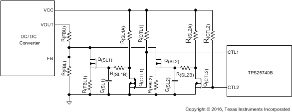
When transition slew control is required, the interaction of the slew mechanism and dc/dc converter loop response must be considered. A simple R-C filter between the device CTL pins and converter feedback node may lead to instability under some conditions. Figure 44 shows a method which controls the slew rate without adding capacitance to the converter feedback node.
 Figure 44. Slew-Rate Control Example No. 1
 When VOUT = 5 V, all CTL pins are in a high impedance state. When a 5 V to 12 V transition is requested, CTL2 goes low and turns off Q(CTL2). Q(SL2) gate starts to rise towards VCC at a rate determined by R(SL2A) + R(SL2B) and C(SL2). Q(SL2) gate continues to rise, until Q(SL2) is fully enhanced placing R(FBL2) in parallel with R(FBL). In similar fashion when C(TL1) goes low, Q(CTL1) turns off allowing R(FBL1) to slew in parallel with R(FBL2) and R(FBL).
The slewing resistors and capacitor can be chosen using the following equations. VT is the VGS threshold voltage of Q(SL1) and Q(SL2). VREF is the feedback regulator reference voltage. Choose the slewing resistance in the 100 kΩ range to reduce the loading on the bias voltage source (VCC) and then calculate C(SL). The falling transitions is shorter than the rising transitions in this topology.
Falling transitions:
- 20 V to 12 V

- 12 V to 5 V

Rising transitions:
- 5 V to 12 V

- 12 V to 20 V

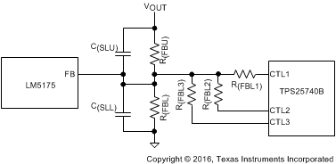
Some converter regulators can tolerate a balance of capacitance on the feedback node without affecting loop stability. The LM5175 has been tested using Figure 45 to combine VOUT slewing with a minimal amount of extra circuitry.
 Figure 45. Slew-Rate Control Example No. 2
 When a higher voltage is requested from TPS25740B, at least one of the CTL pins goes low changing the sensed voltage at the FB pin. The LM5175 compensates by increasing C(SLU). As VOUT increases, C(SLU) is charged at a rate proportional to R(FBU). Three time constants yields a voltage change of approximately 95% and can be used to calculate the desired slew time. C(SLU) can be calculated using Equation 12 and Equation 13.


In order to minimize loop stability effects, a capacitor in parallel with R(FBL) is required. The ratio of C(SLU)/C(SLL) should be chosen to match the ratio of R(FBL)/R(FBU). Choose C(SLL) according to Equation 14.

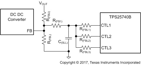
A third slew rate method is shown in Figure 46 using an equivalent resistance, REQ and C(SLL) to provide an exponential slew rate. The slew rate is the derivative of the voltage ramp with the maximum occurring at the beginning of a transition. A DC-DC converter with programmable soft-start can help minimize VOUT overshoot at start-up due to C(SLL). Any VOUT overshoot must decay below V(SOVP5) before TPS25740B applies VBUS in order to prevent OVP shutdown.
 Figure 46. Slew-Rate Control Example No. 3
 For the rising condition, TPS25740B will connect one or more of the R(FBLx) resistors in parallel with C(SLL). The FB node is treated as a virtual ground so that REQ for the rising condition is R(FB1) in parallel with the R(FBLx) resistors being grounded through the CTLx pins. For the falling condition, TPS25740B will disconnect one or more of the R(FBLx) resistors in parallel with C(SLL). REQ for the falling condition is therefore R(FB1) in parallel with the R(FBLx) resistors remaining grounded.

where
- SR = SR(max) at t = 0

The slew rate is proportional to VBUS voltage change and the largest slew rate occurs for the 5 V to 20 V case (or 15 V if 15 V is the highest advertised voltage) where all three R(FBLx) resistors are connected simultaneously. Size C(SLL) for this case using REQ = R(FB1), R(FBL1), R(FBL2), and R(FBL3) in parallel.
For this method, the procedure to choose the voltage programming resistors differs from the examples in section Selection of the CTL1, CTL2, and CTL3 Resistors (R(FBL1), R(FBL2), and R(FBL3)) due to the addition of R(FB1). The TPS25740B Design Calculator Tool (refer to USB PD in 文档支持 ) is available to help with the calculations for this control method. All slew rate control methods should be verified on the bench to ensure that the slew rate requirements are being met when the external VBUS capacitance is between 1 µF and 100 µF.