ZHCSFH8D August   2016  – January 2018 TPS25741 , TPS25741A

UNLESS OTHERWISE NOTED, this document contains PRODUCTION DATA.  

  1. 特性
  2. 应用
  3. 说明
    1.     Device Images
      1.      DFP 主机端口中的简化实施方案
  4. 修订历史记录
  5. Device Comparison Table
  6. Pin Configuration and Functions
    1.     Pin Functions
  7. Specifications
    1. 7.1 Absolute Maximum Ratings
    2. 7.2 ESD Ratings
    3. 7.3 Recommended Operating Conditions
    4. 7.4 Thermal Information
    5. 7.5 Electrical Characteristics
    6. 7.6 Timing Requirements
    7. 7.7 Switching Characteristics
    8. 7.8 Typical Characteristics
  8. Detailed Description
    1. 8.1 Overview
      1. 8.1.1 VBUS Capacitance
      2. 8.1.2 USB Data Communications
    2. 8.2 Functional Block Diagram
    3. 8.3 Feature Description
      1. 8.3.1  USB Type-C CC Logic (CC1, CC2)
      2. 8.3.2  9.3.2 VCONN Supply (VCONN, CC1, CC2)
      3. 8.3.3  USB Power Delivery BMC Transmission (CC1, CC2, VTX)
      4. 8.3.4  USB Power Delivery BMC Reception (CC1, CC2)
      5. 8.3.5  Discharging (DSCG, VPWR)
        1. 8.3.5.1 Discharging after a Fault (VPWR)
      6. 8.3.6  Configuring Voltage Capabilities (HIPWR, EN9V, EN12V)
      7. 8.3.7  Configuring Power Capabilities (PSEL, PCTRL, HIPWR)
      8. 8.3.8  Gate Drivers
        1. 8.3.8.1 GDNG, GDNS
        2. 8.3.8.2 G5V
        3. 8.3.8.3 GDPG
      9. 8.3.9  Fault Monitoring and Protection
        1. 8.3.9.1 Over/Under Voltage (VBUS)
        2. 8.3.9.2 Over-Current Protection (ISNS, VBUS)
        3. 8.3.9.3 System Fault Input (GD, VPWR)
      10. 8.3.10 Voltage Control (CTL1, CTL2)
      11. 8.3.11 Sink Attachment Indicator (UFP, DVDD)
      12. 8.3.12 Accessory Attachment Indicator (AUDIO, DEBUG)
      13. 8.3.13 Plug Polarity Indication (POL)
      14. 8.3.14 Power Supplies (VAUX, VDD, VPWR, DVDD)
      15. 8.3.15 Grounds (AGND, GND)
      16. 8.3.16 Output Power Supply (DVDD)
    4. 8.4 Device Functional Modes
      1. 8.4.1 Sleep Mode
      2. 8.4.2 Checking VBUS at Start Up
  9. Application and Implementation
    1. 9.1 Application Information
      1. 9.1.1 System-Level ESD Protection
      2. 9.1.2 Use of GD Internal Clamp
      3. 9.1.3 Resistor Divider on GD for Programmable Start Up
      4. 9.1.4 Selection of the CTL1 and CTL2 Resistors (RFBL1 and RFBL2)
      5. 9.1.5 Voltage Transition Requirements
      6. 9.1.6 VBUS Slew Control using GDNG CSLEW
      7. 9.1.7 Tuning OCP Using RF and CF
    2. 9.2 Typical Applications
      1. 9.2.1 A/C Multiplexing Power Source
        1. 9.2.1.1 Design Requirements
        2. 9.2.1.2 Detailed Design Procedure
          1. 9.2.1.2.1 Power Pin Bypass Capacitors
          2. 9.2.1.2.2 Non-Configurable Components
          3. 9.2.1.2.3 Configurable Components
        3. 9.2.1.3 Application Curves
      2. 9.2.2 D/C Power Source
        1. 9.2.2.1 Design Requirements
        2. 9.2.2.2 Detailed Design Procedure
          1. 9.2.2.2.1 Power Pin Bypass Capacitors
          2. 9.2.2.2.2 Non-Configurable Components
          3. 9.2.2.2.3 Configurable Components
        3. 9.2.2.3 Application Curves
    3. 9.3 System Examples
      1. 9.3.1 A/C Power Source (Wall Adapter)
      2. 9.3.2 Dual-Port Power Managed A/C Power Source (Wall Adapter)
  10. 10Power Supply Recommendations
    1. 10.1 VDD
    2. 10.2 VCONN
    3. 10.3 VPWR
  11. 11Layout
    1. 11.1 Layout Guidelines
      1. 11.1.1 Port Current Kelvin Sensing
      2. 11.1.2 Power Pin Bypass Capacitors
      3. 11.1.3 Supporting Components
    2. 11.2 Layout Example
  12. 12器件和文档支持
    1. 12.1 Documentation Support
    2. 12.2 相关链接
    3. 12.3 Receiving Notification of Documentation Updates
    4. 12.4 Community Resources
    5. 12.5 商标
    6. 12.6 静电放电警告
    7. 12.7 Glossary
  13. 13机械、封装和可订购信息

封装选项

机械数据 (封装 | 引脚)
散热焊盘机械数据 (封装 | 引脚)
订购信息

Typical Characteristics

TPS25741 TPS25741A D004_SLVSDG8.gif
IDSCG = 100 mA
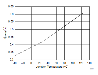
Figure 7. VDSCG when VPWR > 4.65 V
TPS25741 TPS25741A D009_SLVSDJ5.gif
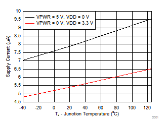
CC pins are open
Figure 9. Supply Current when VPWR = 5 V
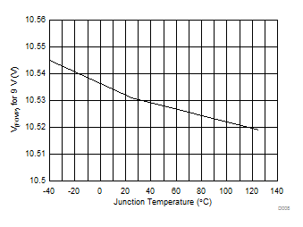
TPS25741 TPS25741A D008_SLVSDG8.gif
Figure 11. VFOVP While Supplying 9 V, TPS25741A
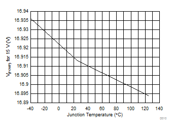
TPS25741 TPS25741A D010_SLVSDG8.gif
Figure 13. VFOVP While Supplying 15 V, TPS25741A
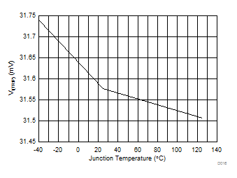
TPS25741 TPS25741A D016_SLVSDG8.gif
5 A enabled
Figure 15. VITRIP When VPWR> 4.65 V
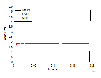
TPS25741 TPS25741A D012_SLVSDG8.gif
Sink attached at time 0
UFP pulled up to DVDD
Figure 17. DVDD and UFP Upon Sink Attachment
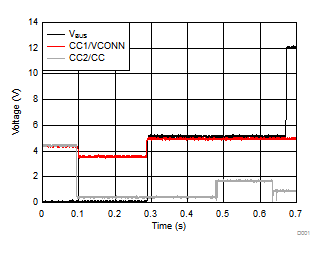
TPS25741 TPS25741A D020_SLVSDJ5.gif
VDD = 5 V
Figure 19. VBUS, CC1, and CC2 Upon Attachment
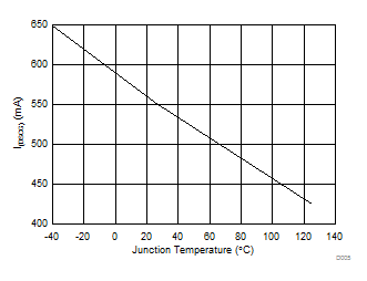
TPS25741 TPS25741A D005_SLVSDG8.gif
VDSCG = 4 V pulsed testing
Figure 8. IDSCG when VPWR> 4.65 V
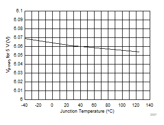
TPS25741 TPS25741A D007_SLVSDG8.gif
Figure 10. VFOVP While Supplying 5 V
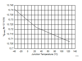
TPS25741 TPS25741A D009_SLVSDG8.gif
Figure 12. VFOVP While Supplying 12 V, TPS25741
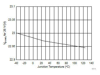
TPS25741 TPS25741A D015_SLVSDG8.gif
Figure 14. VFOVP While Supplying 20 V, TPS25741
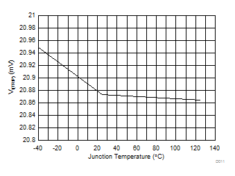
TPS25741 TPS25741A D011_SLVSDG8.gif
3 A enabled
Figure 16. VITRIP When VPWR> 4.65 V
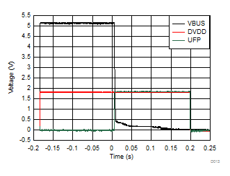
TPS25741 TPS25741A D013_SLVSDG8.gif
Sink detached at time 0.19s
Sleep mode entered at time 0.39s.
UFP pulled up to DVDD
Figure 18. DVDD and UFP Upon Sink Attachment