ZHCSFH8D August 2016 – January 2018 TPS25741 , TPS25741A
UNLESS OTHERWISE NOTED, this document contains PRODUCTION DATA.
- 1 特性
- 2 应用
- 3 说明
- 4 修订历史记录
- 5 Device Comparison Table
- 6 Pin Configuration and Functions
- 7 Specifications
-
8 Detailed Description
- 8.1 Overview
- 8.2 Functional Block Diagram
- 8.3
Feature Description
- 8.3.1 USB Type-C CC Logic (CC1, CC2)
- 8.3.2 9.3.2 VCONN Supply (VCONN, CC1, CC2)
- 8.3.3 USB Power Delivery BMC Transmission (CC1, CC2, VTX)
- 8.3.4 USB Power Delivery BMC Reception (CC1, CC2)
- 8.3.5 Discharging (DSCG, VPWR)
- 8.3.6 Configuring Voltage Capabilities (HIPWR, EN9V, EN12V)
- 8.3.7 Configuring Power Capabilities (PSEL, PCTRL, HIPWR)
- 8.3.8 Gate Drivers
- 8.3.9 Fault Monitoring and Protection
- 8.3.10 Voltage Control (CTL1, CTL2)
- 8.3.11 Sink Attachment Indicator (UFP, DVDD)
- 8.3.12 Accessory Attachment Indicator (AUDIO, DEBUG)
- 8.3.13 Plug Polarity Indication (POL)
- 8.3.14 Power Supplies (VAUX, VDD, VPWR, DVDD)
- 8.3.15 Grounds (AGND, GND)
- 8.3.16 Output Power Supply (DVDD)
- 8.4 Device Functional Modes
- 9 Application and Implementation
- 10Power Supply Recommendations
- 11Layout
- 12器件和文档支持
- 13机械、封装和可订购信息
9.1.6 VBUS Slew Control using GDNG CSLEW
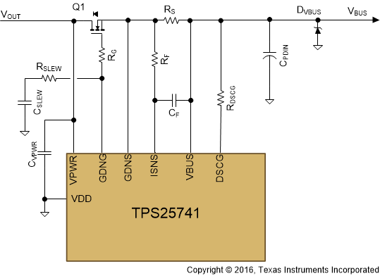
Care should be taken to control the slew rate of Q1 using CSLEW; particularly in applications where COUT>> CSLEW. The slew rate observed on VBUS when charging a purely capacitive load is the same as the slew rate of VGDNG and is dominated by the ratio IGDNGON /CSLEW. RSLEW helps block CSLEW from the GDNG pin enabling a faster transient response to OCP.
 Figure 48. Slew-Rate Control Using GDNG
There may be fault conditions where the voltage on VBUS triggers an OVP condition and then remains at a high voltage even after the TPS25741 configures the voltage source to output 5 V via CTL1 and CTL2. When this OVP occurs, the TPS25741 opens Q1 within tFOVP + tFOVPDG. The TPS25741 then issues a hard reset, discharges the power-path via the RDSCG, and waits for 795 ms before enabling Q1 again. Due to the fault condition the voltage again triggers an OVP event when the voltage on VBUS exceeds VFOVP. This retry process would continue as long as the fault condition persists, periodically pulsing up to VFOVP + VSrcSlewPos x (tFOVP + tFOVPDG) onto the VBUS of the Type-C receptacle. It is recommended to use a slew rate less than the maximum of VSrcSlewPos (30 mV/µs), refer to Documentation Support section, the slew rate should instead be set in order to meet the requirement to have the voltage reach the target voltage within tSrcSettle (275 ms) (refer to USB Power Delivery in Documentation Support). This also limits the out-rush current from the COUT capacitor into the CPDIN capacitor and helps protect Q1 and RS.