ZHCSTM4A October   2023  – March 2024 TPS25751

PRODUCTION DATA  

  1.   1
  2. 特性
  3. 应用
  4. 说明
  5. Device Comparison Table
  6. Pin Configuration and Functions
  7. Specifications
    1. 6.1  Absolute Maximum Ratings
      1. 6.1.1 TPS25751D and TPS25751S - Absolute Maximum Ratings
      2. 6.1.2 TPS25751D - Absolute Maximum Ratings
      3. 6.1.3 TPS25751S - Absolute Maximum Ratings
    2. 6.2  ESD Ratings
    3. 6.3  Recommended Operating Conditions
      1. 6.3.1 TPS25751D - Recommended Operating Conditions
      2. 6.3.2 TPS25751S - Recommended Operating Conditions
    4. 6.4  Recommended Capacitance
    5. 6.5  Thermal Information
      1. 6.5.1 TPS25751D - Thermal Information
      2. 6.5.2 TPS25751S - Thermal Information
    6. 6.6  Power Supply Characteristics
    7. 6.7  Power Consumption
    8. 6.8  PP_5V Power Switch Characteristics
    9. 6.9  PPHV Power Switch Characteristics - TPS25751D
    10. 6.10 PP_EXT Power Switch Characteristics - TPS25751S
    11. 6.11 Power Path Supervisory
    12. 6.12 CC Cable Detection Parameters
    13. 6.13 CC VCONN Parameters
    14. 6.14 CC PHY Parameters
    15. 6.15 Thermal Shutdown Characteristics
    16. 6.16 ADC Characteristics
    17. 6.17 Input/Output (I/O) Characteristics
    18. 6.18 BC1.2 Characteristics
    19. 6.19 I2C Requirements and Characteristics
    20. 6.20 Typical Characteristics
  8. Parameter Measurement Information
  9. Detailed Description
    1. 8.1 Overview
    2. 8.2 Functional Block Diagram
    3. 8.3 Feature Description
      1. 8.3.1  USB-PD Physical Layer
        1. 8.3.1.1 USB-PD Encoding and Signaling
        2. 8.3.1.2 USB-PD Bi-Phase Marked Coding
        3. 8.3.1.3 USB-PD Transmit (TX) and Receive (Rx) Masks
        4. 8.3.1.4 USB-PD BMC Transmitter
        5. 8.3.1.5 USB-PD BMC Receiver
        6. 8.3.1.6 Squelch Receiver
      2. 8.3.2  Power Management
        1. 8.3.2.1 Power-On And Supervisory Functions
        2. 8.3.2.2 VBUS LDO
      3. 8.3.3  Power Paths
        1. 8.3.3.1 Internal Sourcing Power Paths
          1. 8.3.3.1.1 PP_5V Current Clamping
          2. 8.3.3.1.2 PP_5V Local Overtemperature Shut Down (OTSD)
          3. 8.3.3.1.3 PP_5V OVP
          4. 8.3.3.1.4 PP_5V UVLO
          5. 8.3.3.1.5 PP_5Vx Reverse Current Protection
          6. 8.3.3.1.6 PP_CABLE Current Clamp
          7. 8.3.3.1.7 PP_CABLE Local Overtemperature Shut Down (OTSD)
          8. 8.3.3.1.8 PP_CABLE UVLO
        2. 8.3.3.2 TPS25751D Internal Sink Path
          1. 8.3.3.2.1 Overvoltage Protection (OVP)
          2. 8.3.3.2.2 Reverse-Current Protection (RCP)
          3. 8.3.3.2.3 VBUS UVLO
          4. 8.3.3.2.4 Discharging VBUS to Safe Voltage
        3. 8.3.3.3 TPS25751S - External Sink Path Control PP_EXT
          1. 8.3.3.3.1 Overvoltage Protection (OVP)
            1. 8.3.3.3.1.1 Reverse-Current Protection (RCP)
            2. 8.3.3.3.1.2 VBUS UVLO
            3. 8.3.3.3.1.3 Discharging VBUS to Safe Voltage
      4. 8.3.4  Cable Plug and Orientation Detection
        1. 8.3.4.1 Configured as a Source
        2. 8.3.4.2 Configured as a Sink
        3. 8.3.4.3 Configured as a DRP
        4. 8.3.4.4 Dead Battery Advertisement
      5. 8.3.5  Overvoltage Protection (CC1, CC2)
      6. 8.3.6  Default Behavior Configuration (ADCIN1, ADCIN2)
      7. 8.3.7  ADC
      8. 8.3.8  BC 1.2 (USB_P, USB_N)
      9. 8.3.9  Digital Interfaces
        1. 8.3.9.1 General GPIO
        2. 8.3.9.2 I2C Interface
      10. 8.3.10 Digital Core
      11. 8.3.11 I2C Interface
        1. 8.3.11.1 I2C Interface Description
          1. 8.3.11.1.1 I2C Clock Stretching
          2. 8.3.11.1.2 I2C Address Setting
          3. 8.3.11.1.3 Unique Address Interface
    4. 8.4 Device Functional Modes
      1. 8.4.1 Pin Strapping to Configure Default Behavior
      2. 8.4.2 Power States
    5. 8.5 Thermal Shutdown
  10. Application and Implementation
    1. 9.1 Application Information
    2. 9.2 Typical Application
      1. 9.2.1 Design Requirements
        1. 9.2.1.1 Programmable Power Supply (PPS) - Design Requirements
        2. 9.2.1.2 Liquid Detection Design Requirements
        3. 9.2.1.3 BC1.2 Application Design Requirements
        4. 9.2.1.4 USB Data Support Design Requirements
      2. 9.2.2 Detailed Design Procedure
        1. 9.2.2.1 Programmable Power Supply (PPS)
        2. 9.2.2.2 Liquid Detection
          1. 9.2.2.2.1 Liquid Detection Operation
        3. 9.2.2.3 BC1.2 Application
        4. 9.2.2.4 USB Data Support
      3. 9.2.3 Application Curves
        1. 9.2.3.1 Programmable Power Supply (PPS) Application Curves
        2. 9.2.3.2 Liquid Detection Application Curves
        3. 9.2.3.3 BC1.2 Application Curves
        4. 9.2.3.4 USB Data Support Application Curves
    3. 9.3 Power Supply Recommendations
      1. 9.3.1 3.3-V Power
        1. 9.3.1.1 VIN_3V3 Input Switch
      2. 9.3.2 1.5-V Power
      3. 9.3.3 Recommended Supply Load Capacitance
    4. 9.4 Layout
      1. 9.4.1 TPS25751D - Layout
        1. 9.4.1.1 Layout Guidelines
          1. 9.4.1.1.1 Recommended Via Size
          2. 9.4.1.1.2 Minimum Trace Widths
        2. 9.4.1.2 Layout Example
          1. 9.4.1.2.1 TPS25751D Schematic Layout Example
          2. 9.4.1.2.2 TPS25751D Layout Example - PCB Plots
            1. 9.4.1.2.2.1 TPS25751D Component Placement
            2. 9.4.1.2.2.2 TPS25751D PP5V
            3. 9.4.1.2.2.3 TPS25751D PPHV
            4. 9.4.1.2.2.4 TPS25751D VBUS
            5. 9.4.1.2.2.5 TPS25751D I/O (I2C, ADCINs, GPIOs)
            6. 9.4.1.2.2.6 TPS25751D DRAIN
            7. 9.4.1.2.2.7 TPS25751D GND
      2. 9.4.2 TPS25751S - Layout
        1. 9.4.2.1 Layout Guidelines
          1. 9.4.2.1.1 Recommended Via Size
          2. 9.4.2.1.2 Minimum Trace Widths
        2. 9.4.2.2 Layout Example
          1. 9.4.2.2.1 TPS25751S Schematic Layout Example
          2. 9.4.2.2.2 TPS25751S Layout Example - PCB Plots
            1. 9.4.2.2.2.1 TPS25751S Component Placement
            2. 9.4.2.2.2.2 TPS25751S PP5V
            3. 9.4.2.2.2.3 TPS25751S PP_EXT
            4. 9.4.2.2.2.4 TPS25751S VBUS
            5. 9.4.2.2.2.5 TPS25751S I/O
            6. 9.4.2.2.2.6 TPS25751S PPEXT Gate Driver
            7. 9.4.2.2.2.7 TPS25751S GND
  11. 10Device and Documentation Support
    1. 10.1 Device Support
      1. 10.1.1 第三方米6体育平台手机版_好二三四免责声明
      2. 10.1.2 Firmware Warranty Disclaimer
    2. 10.2 Documentation Support
      1. 10.2.1 Related Documentation
    3. 10.3 接收文档更新通知
    4. 10.4 支持资源
    5. 10.5 Trademarks
    6. 10.6 静电放电警告
    7. 10.7 术语表
  12. 11Revision History
  13. 12Mechanical, Packaging, and Orderable Information

封装选项

机械数据 (封装 | 引脚)
散热焊盘机械数据 (封装 | 引脚)
订购信息

Power Management

The TPS25751 power management block receives power and generates voltages to provide power to the TPS25751 internal circuitry. These generated power rails are LDO_3V3 and LDO_1V5. LDO_3V3 can also be used as a low power output for external EEPROM memory. The power supply path is shown in Figure 8-11.
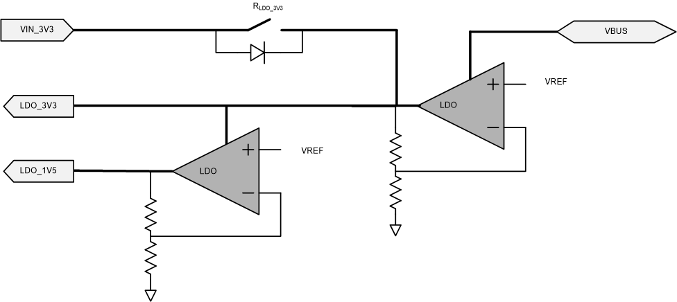
GUID-0F78F003-5EA9-475E-8C1B-DF20B9D9CF55-low.gifFigure 8-11 Power Supplies

The TPS25751 is powered from either VIN_3V3 or VBUS. The normal power supply input is VIN_3V3. When powering from VIN_3V3, current flows from VIN_3V3 to LDO_3V3 to power the core 3.3-V circuitry and I/Os. A second LDO steps the voltage down from LDO_3V3 to LDO_1V5 to power the 1.5-V core digital circuitry. When VIN_3V3 power is unavailable and power is available on VBUS, it is referred to as the dead-battery start-up condition. In a dead-battery start-up condition, the TPS25751 opens the VIN_3V3 switch until the host clears the dead-battery flag through I2C. Therefore, the TPS25751 is powered from the VBUS input with the higher voltage during the dead-battery start-up condition and until the dead-battery flag is cleared. When powering from a VBUS input, the voltage on VBUS is stepped down through an LDO to LDO_3V3.