ZHCSP87A December 2022 – September 2023 TPS25772-Q1
PRODUCTION DATA
- 1
- 1 特性
- 2 应用
- 3 说明
- 4 Revision History
- 5 Device Comparison Table
- 6 Pin Configuration and Functions
-
7 Specifications
- 7.1 Absolute Maximum Ratings
- 7.2 ESD Ratings
- 7.3 Recommended Operating Conditions
- 7.4 Recommended Components
- 7.5 Thermal Information
- 7.6 Buck-Boost Regulator
- 7.7 CC Cable Detection Parameters
- 7.8 CC VCONN Parameters
- 7.9 CC PHY Parameters
- 7.10 Thermal Shutdown Characteristics
- 7.11 Oscillator Characteristics
- 7.12 ADC Characteristics
- 7.13 TVS Parameters
- 7.14 Input/Output (I/O) Characteristics
- 7.15 BC1.2 Characteristics
- 7.16 I2C Requirements and Characteristics
- 7.17 Typical Characteristics
- 8 Parameter Measurement Information
-
9 Detailed Description
- 9.1 Overview
- 9.2 Functional Block Diagram
- 9.3
Feature Description
- 9.3.1 Device Power Management and Supervisory Circuitry
- 9.3.2 TVSP Device Configuration and ESD Protection
- 9.3.3
Buck-Boost Regulator
- 9.3.3.1 Buck-Boost Regulator Operation
- 9.3.3.2 Switching Frequency, Frequency Dither, Phase-Shift and Synchronization
- 9.3.3.3 VIN Supply and VIN Over-Voltage Protection
- 9.3.3.4 Feedback Paths and Error Amplifiers
- 9.3.3.5 Transconductors and Compensation
- 9.3.3.6 Output Voltage DAC, Soft-Start and Cable Droop Compensation
- 9.3.3.7 VBUS Overvoltage Protection
- 9.3.3.8 VBUS Undervoltage Protection
- 9.3.3.9 Current Sense Resistor (RSNS) and Current Limit Operation
- 9.3.3.10 Buck-Boost Peak Current Limits
- 9.3.4 USB-PD Physical Layer
- 9.3.5 VCONN
- 9.3.6 Cable Plug and Orientation Detection
- 9.3.7 ADC
- 9.3.8 BC 1.2, Legacy and Fast Charging Modes (Px_DP, Px_DM)
- 9.3.9 USB2.0 Low-Speed Endpoint
- 9.3.10 Digital Interfaces
- 9.3.11 I2C Interface
- 9.3.12 Digital Core
- 9.3.13 NTC Input
- 9.3.14 Thermal Sensors and Thermal Shutdown
- 9.4 Device Functional Modes
- 10Application and Implementation
- 11Device and Documentation Support
- 12Mechanical, Packaging, and Orderable Information
8 Parameter Measurement Information
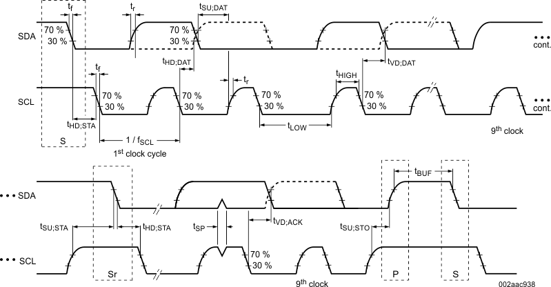
 Figure 8-1 I2C Slave Interface Timing
 Figure 8-2 GPIO Output Timing Diagram (rise/fall vs capacitive load)
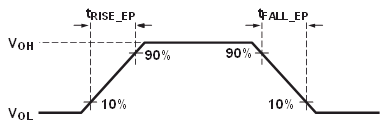
 Figure 8-3 USB Endpoint
Transmitter Rise and Fall Time
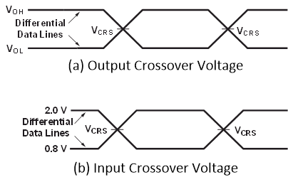
 Figure 8-4 USB Endpoint Crossover
Voltages