ZHCSP87A December 2022 – September 2023 TPS25772-Q1
PRODUCTION DATA
- 1
- 1 特性
- 2 应用
- 3 说明
- 4 Revision History
- 5 Device Comparison Table
- 6 Pin Configuration and Functions
-
7 Specifications
- 7.1 Absolute Maximum Ratings
- 7.2 ESD Ratings
- 7.3 Recommended Operating Conditions
- 7.4 Recommended Components
- 7.5 Thermal Information
- 7.6 Buck-Boost Regulator
- 7.7 CC Cable Detection Parameters
- 7.8 CC VCONN Parameters
- 7.9 CC PHY Parameters
- 7.10 Thermal Shutdown Characteristics
- 7.11 Oscillator Characteristics
- 7.12 ADC Characteristics
- 7.13 TVS Parameters
- 7.14 Input/Output (I/O) Characteristics
- 7.15 BC1.2 Characteristics
- 7.16 I2C Requirements and Characteristics
- 7.17 Typical Characteristics
- 8 Parameter Measurement Information
-
9 Detailed Description
- 9.1 Overview
- 9.2 Functional Block Diagram
- 9.3
Feature Description
- 9.3.1 Device Power Management and Supervisory Circuitry
- 9.3.2 TVSP Device Configuration and ESD Protection
- 9.3.3
Buck-Boost Regulator
- 9.3.3.1 Buck-Boost Regulator Operation
- 9.3.3.2 Switching Frequency, Frequency Dither, Phase-Shift and Synchronization
- 9.3.3.3 VIN Supply and VIN Over-Voltage Protection
- 9.3.3.4 Feedback Paths and Error Amplifiers
- 9.3.3.5 Transconductors and Compensation
- 9.3.3.6 Output Voltage DAC, Soft-Start and Cable Droop Compensation
- 9.3.3.7 VBUS Overvoltage Protection
- 9.3.3.8 VBUS Undervoltage Protection
- 9.3.3.9 Current Sense Resistor (RSNS) and Current Limit Operation
- 9.3.3.10 Buck-Boost Peak Current Limits
- 9.3.4 USB-PD Physical Layer
- 9.3.5 VCONN
- 9.3.6 Cable Plug and Orientation Detection
- 9.3.7 ADC
- 9.3.8 BC 1.2, Legacy and Fast Charging Modes (Px_DP, Px_DM)
- 9.3.9 USB2.0 Low-Speed Endpoint
- 9.3.10 Digital Interfaces
- 9.3.11 I2C Interface
- 9.3.12 Digital Core
- 9.3.13 NTC Input
- 9.3.14 Thermal Sensors and Thermal Shutdown
- 9.4 Device Functional Modes
- 10Application and Implementation
- 11Device and Documentation Support
- 12Mechanical, Packaging, and Orderable Information
9.3.2 TVSP Device Configuration and ESD Protection
The Transient Voltage protection and firmware Setting Pin (TVSP) has three functions: 1) Boot configuration settings; 2) USB connector pin short to VBUS or VBAT protection; and 3) USB connector pin enhanced ESD protection.
- RTVSP: At power on, the resistance between the TVSP pin and PGND determines the boot method, USB PD port I2C addresses and I2C logic thresholds. Refer to Table 9-4 and Table 9-5. The most common configuration is shown in Figure 9-4 with RTVSP open, corresponding to TVSP Index 0. During device initialization and boot, typically within 4 seconds after power on, VIN must be above 7.6 V to ensure proper bias of the TVSP pin to 5.5 V. Once boot is complete the device can operate over the full VIN range.
- CTVSP: A 0.1-µF capacitor (CTVSP) must be connected to PGND. Place CTVSP as close to the TVSP pin as possible to minimize parasitic inductance. CTVSP is part of the centralized protection circuitry fortifying connector pins Px_CCy, Px_DP and Px_DM from damage during short to VBUS, VBAT and ESD events. A 40-V 0.1-µF capacitor is recommended for proper operation of the internal TVSP regulator circuit.
- TVSP Damper Network:
Capacitance, CDAMP, and resistance, RDAMP, form an RC
network preventing excessive current from flowing inside the device durging
connector pin over-voltage and ESD events.
- CDAMP: A 0.47-µF capacitor must be connected in series with RDAMP to PGND. A 40-V 0.47-µF capacitor is recommended.
- RDAMP: A 10-Ω resistor must be connected in series with CDAMP to PGND. A 0.25-W rating is recommended.
 Figure 9-4 Basic TVSP Pin
Connection
Figure 9-4 Basic TVSP Pin
Connection| CTVSP | RDAMP | CDAMP |
|---|---|---|
| 0.1 μF | 10 Ω | 0.47 μF |
| RTVSP (kΩ) (1) | TVSP Index | ADC Value | I2C Target Port Addresses (A | B)(2) | I2C Logic (VDD) | Boot Mode |
|---|---|---|---|---|---|
| Open | 0 | ≤ 10 (0x0A) | 0x22 | 0x26 | 3.3 V | EEPROM |
| 93.1 | 1 | ≤ 24 (0x18) | 0x23 | 0x27 | 3.3 V | External HUB/MCU |
| 47.5 | 2 | ≤ 42 (0x2A) | 0x22 | 0x26 | 1.8 V | EEPROM |
| 29.4 | 3 | ≤ 63 (0x3F) | 0x23 | 0x27 | 1.8 V | External HUB/MCU |
| 20.0 | 4 | ≤ 89 (0x59) | 0x23 | 0x27 | 3.3 V | EEPROM |
| 14.7 | 5 | ≤ 119 (0x77) | 0x22 | 0x26 | 3.3 V | External HUB/MCU |
| 11.0 | 6 | ≤ 156 (0x9C) | 0x23 | 0x27 | 1.8 V | EEPROM |
| 8.45 | 7 | ≤ 201 (0xC9) | 0x22 | 0x26 | 1.8 V | External HUB/MCU |
| 6.65 | 8 | ≤ 255 (0xFF) | 0x22 | 0x26 | 3.3 V | Firmware Update |
| RTVSP (kΩ)(1) | TVSP Index | ADC Value | I2C Target Port Addresses (A | B)(2) | I2C Logic (VDD) | Boot Mode |
|---|---|---|---|---|---|
| Open | 0 | ≤ 201 (0x0A) | 0x22 | 0x26 | 3.3 V | EEPROM |
| 5.6 | 8 | ≤ 255 (0xFF) | 0x22 | 0x26 | 3.3 V | Firmware Update |
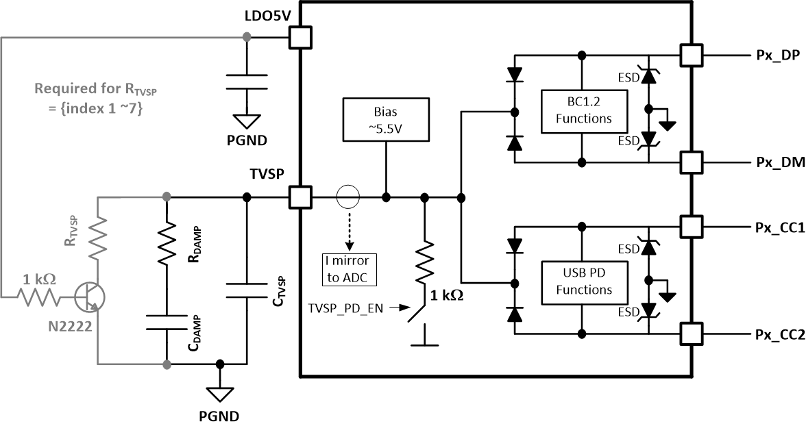
Applications requiring a configuration other than standard, TVSP Index 0 (RTVSP open), as shown in Table 9-4 must implement a circuit similar to the one shown in Figure 9-5. The base of the bipolar transistor is connected to LDO_5V to provide proper power up sequencing of the TVSP resistor - OFF when TPS25772-Q1 is disabled and ON when TPS25772-Q1 is enabled. A 2N2222 is recommended for its large collector-emitter breakdown voltage, low-cost and wide availability.
 Figure 9-5 RTVSP Circuit
Configuration
Figure 9-5 RTVSP Circuit
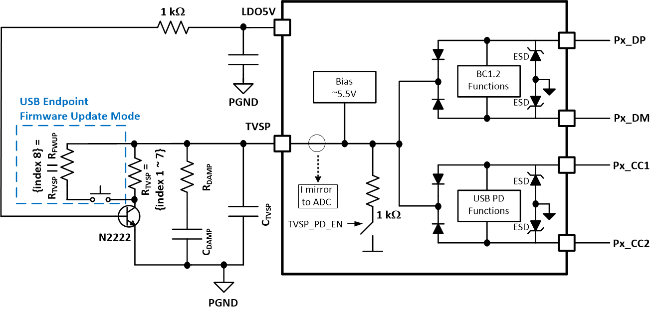
ConfigurationDevice firmware can be updated using the USB Endpoint on the PA_DP and PA_DM pins. To enable firmware update mode, boot the device with a resistance corresponding to Index 8 between TVPS and PGND. A boot cycle can be performed by power cycling the device or by pulling the EN/UVLO pin momentarily below VEN(OPER) threshold. An example circuit to enable USB Endpoint firmware update mode is shown in Figure 9-6
 Figure 9-6 Example Circuit to Enable USB
Endpoint Firmware Update Mode