ZHCSE73C September 2015 – July 2017 TPS25810
PRODUCTION DATA.
- 1 特性
- 2 应用
- 3 说明
- 4 修订历史记录
- 5 Pin Configuration and Functions
- 6 Specifications
-
7 Detailed Description
- 7.1 Overview
- 7.2 Functional Block Diagram
- 7.3
Feature Description
- 7.3.1 Configuration Channel Pins CC1 and CC2
- 7.3.2 Current Capability Advertisement and Overload Protection
- 7.3.3
Undervoltage Lockout (UVLO)
- 7.3.3.1 Device Power Pins (IN1, IN2, AUX, OUT, and GND)
- 7.3.3.2 FAULT Response
- 7.3.3.3 Thermal Shutdown
- 7.3.3.4 REF
- 7.3.3.5 Audio Accessory Detection
- 7.3.3.6 Debug Accessory Detection
- 7.3.3.7 Plug Polarity Detection
- 7.3.3.8 Device Enable Control
- 7.3.3.9 Load Detect
- 7.3.3.10 Power Wake
- 7.3.3.11 Port Power Management (PPM)
- 7.3.3.12 Implementing PPM in a System with Two Type-C Ports
- 7.3.3.13 PPM Operation
- 7.4 Device Functional Modes
- 8 Application and Implementation
- 9 Power Supply Recommendations
- 10Layout
- 11器件和文档支持
- 12机械、封装和可订购信息
6 Specifications
6.1 Absolute Maximum Ratings
over operating free-air temperature range, voltages are respect to GND (unless otherwise noted) (1)| MIN | MAX | UNIT | ||
|---|---|---|---|---|
| Pin voltage, V | IN1, IN2, AUX, EN, CHG, CHG_HI, REF, OUT, LD_DET, FAULT, CC1, CC2, UFP, POL, AUDIO, DEBUG | –0.3 | 7 | V |
| REF_RTN | Internally connected to GND | V | ||
| Pin positive source current, ISRC | OUT, REF, CC1, CC2 | Internally limited | A | |
| Pin positive sink current, ISNK | OUT (while applying VBUS) | 5 | A | |
| CC1, CC2 (while applying VCONN) | 1 | A | ||
| LD_DET, FAULT, UFP, POL, AUDIO, DEBUG | Internally limited | mA | ||
| Operating junction temperature, TJ | –40 | 180 | °C | |
| Storage temperature range, Tstg | –65 | 150 | °C | |
(1) Stresses beyond those listed under Absolute Maximum Ratings may cause permanent damage to the device. These are stress ratings only, which do not imply functional operation of the device at these or any other conditions beyond those indicated under Recommended Operating Conditions. Exposure to absolute-maximum-rated conditions for extended periods may affect device reliability.
6.2 ESD Ratings
| VALUE | UNIT | ||||
|---|---|---|---|---|---|
| V(ESD)(1) | Electrostatic discharge | Human-body model (HBM), per ANSI/ESDA/JEDEC JS-001(2) | ±2000 | V | |
| Charged-device model (CDM), per JEDEC specification JESD22-C101(3) | ±500 | ||||
| IEC(4) | IEC61000-4-2 contact discharge, CC1 and CC2 | ±8000 | |||
| IEC61000-4-2 air discharge, CC1 and CC2 | ±15000 | ||||
(1) Electrostatic discharge (ESD) to measure device sensitivity/immunity to damage caused by assembly line electrostatic discharges into the device.
(2) JEDEC document JEP155 states that 500-V HBM allows safe manufacturing with a standard ESD control process.
(3) JEDEC document JEP157 states that 250-V CDM allows safe manufacturing with a standard ESD control process.
(4) Surges per IEC61000-402, 1999 applied between CC1/CC2 and output ground of the TPS25810EVM-745.
6.3 Recommended Operating Conditions
Voltages are with respect to GND (unless otherwise noted)| MIN | NOM | MAX | UNIT | |||
|---|---|---|---|---|---|---|
| VI | Supply voltage | IN1 | 4.5 | 6.5 | V | |
| IN2 | 4.5 | 5.5 | ||||
| AUX | 2.9 | 5.5 | ||||
| VI | Input voltage | EN, CHG, CHG_HI | 0 | 5.5 | V | |
| VIH | High-level input voltage | EN, CHG, CHG_HI | 1.17 | V | ||
| VIL | Low-level voltage | EN, CHG, CHG_HI | 0.63 | V | ||
| VPU | Pull-up voltage | Used on LD_DET, FAULT, UFP, POL, AUDIO, DEBUG | 0 | 5.5 | V | |
| ISRC | Positive source current | OUT | 3 | A | ||
| CC1 or CC2 when supplying VCONN | 250 | mA | ||||
| ISNK | Positive sink current (10 ms moving average) | LD_DET, FAULT, UFP, POL, AUDIO, DEBUG | 10 | mA | ||
| ISNK_PULSE | Positive repetitive pulse sink current | LD_DET, FAULT, UFP, POL, AUDIO, DEBUG | Internally Limited | mA | ||
| RREF | Reference Resistor | 98 | 100 | 102 | kΩ | |
| TJ | Operating junction temperature | –40 | 125 | °C | ||
6.4 Thermal Information
| THERMAL METRIC(1) | TPS25810 | UNIT | |
|---|---|---|---|
| RVC (WQFN) | |||
| 20 PINS | |||
| RθJA | Junction-to-ambient thermal resistance | 39.3 | °C/W |
| RθJC(top) | Junction-to-case (top) thermal resistance | 43.4 | °C/W |
| RθJB | Junction-to-board thermal resistance | 13 | °C/W |
| ψJT | Junction-to-top characterization parameter | 0.7 | °C/W |
| ψJB | Junction-to-board characterization parameter | 13 | °C/W |
| RθJC(bot) | Junction-to-case (bottom) thermal resistance | 4.2 | °C/W |
(1) For more information about traditional and new thermal metrics, see the Semiconductor and IC Package Thermal Metrics application report.
6.5 Electrical Characteristics
–40°C ≤ TJ ≤ 125°C, 4.5 V ≤ VIN1 ≤ 6.5 V, 4.5 V ≤ VIN2 ≤ 5.5 V, 2.9 V ≤ VAUX ≤ 5.5 V; VEN = VCHG = VCHG_HI = VAUX, RREF = 100 kΩ. Typical values are at 25°C. All voltages are with respect to GND. IOUT and IOS defined positive out of the indicated pin (unless otherwise noted)| PARAMETER | TEST CONDITIONS | MIN | TYP | MAX | UNIT | |
|---|---|---|---|---|---|---|
| OUT - POWER SWITCH | ||||||
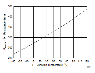
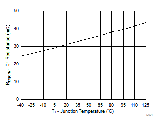
| RDS(on) | On resistance(1) | TJ = 25°C, IOUT = 3 A | 34 | 37 | mΩ | |
| –40°C ≤ TJ ≤ 85°C, IOUT = 3 A | 34 | 46 | ||||
| –40°C ≤ TJ ≤ 125°C, IOUT = 3 A | 34 | 55 | ||||
| IREV | OUT to IN reverse leakage current | VOUT = 6.5 V, VIN1 = VEN = 0 V, –40°C ≤ TJ ≤ 85°C, IREV is current out of IN1 pin |
0 | 3 | µA | |
| OUT - CURRENT LIMIT | ||||||
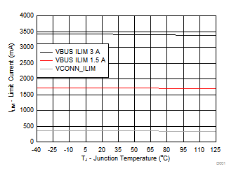
| IOS | Short circuit current limit (1) | VCHG = 0 V or VCHG = VAUX and VCHG_HI = 0 V | 1.58 | 1.7 | 1.82 | A |
| VCHG = VAUX and VCHG_HI = VAUX | 3.16 | 3.4 | 3.64 | |||
| RREF = 10 Ω | 7 | |||||
| OUT - DISCHARGE | ||||||
| Discharge resistance | VOUT = 4 V, UFP signature removed from CC lines, time < tw_DCHG | 400 | 500 | 600 | Ω | |
| Bleed discharge resistance | VOUT = 4 V, No UFP signature on CC lines, time > tw_DCHG | 100 | 150 | 250 | kΩ | |
| REF | ||||||
| VO | Output voltage | 0.78 | 0.8 | 0.82 | V | |
| IOS | Short circuit current | RREF = 10 Ω | 9.5 | 15.3 | µA | |
| FAULT | ||||||
| VOL | Output low voltage | IFAULT = 1 mA | 350 | mV | ||
| IOFF | Off-state leakage | VFAULT = 5.5 V | 1 | µA | ||
| LD_DET | ||||||
| VOL | Output low voltage | ILD_DET = 1 mA | 350 | mV | ||
| IOFF | Off-state leakage | VLD_DET = 5.5 V | 1 | µA | ||
| ITH | OUT sourcing, rising threshold current for load detect | 1.8 | 1.95 | 2.1 | A | |
| Hysteresis(2) | 125 | mA | ||||
| CC1/CC2 - VCONN POWER SWITCH | ||||||
| RDS(on) | On resistance | TJ = 25°C, IOUT = 250 mA | 365 | 420 | mΩ | |
| -40°C ≤ TJ ≤ 85°C, IOUT = 250 mA | 365 | 530 | ||||
| -40°C ≤ TJ ≤ 125°C, IOUT = 250 mA | 365 | 600 | ||||
| CC1/CC2 - VCONN POWER SWITCH - CURRENT LIMIT | ||||||
| IOS | Short circuit current limit(1) | 300 | 355 | 410 | mA | |
| RREF = 10 Ω | 800 | |||||
| CC1/CC2 – CONNECT MANAGEMENT – DANGLING ELECTRONICALLY MARKED CABLE MODE | ||||||
| ISRC | Sourcing current on the pass-through CC Line | 0 V ≤ VCCx ≤ 1.5 V | 64 | 80 | 96 | µA |
| Sourcing current on the Ra CC line | 0 V ≤ VCCx ≤ 1.5 V | 64 | 80 | 96 | µA | |
| CC1/CC2 – CONNECT MANAGEMENT – ACCESSORY MODE | ||||||
| ISRC | CCx Sourcing current (CC2- Audio, CC1-Debug) |
0 V ≤ VCCx ≤ 1.5 V | 64 | 80 | 96 | µA |
| CCx Sourcing current (CC1- Audio, CC2-Debug) (2) |
0 V ≤ VCCx ≤ 1.5 V | 0 | µA | |||
| CC1/CC2 – CONNECT MANAGEMENT – UFP MODE | ||||||
| ISRC | Sourcing current with either IN1 or IN2 in UVLO | 0 V ≤ VCCx ≤ 1.5 V VIN1 < VTH_UVLO_IN1 or VIN2 < VTH_UVLO_IN2 |
64 | 80 | 96 | µA |
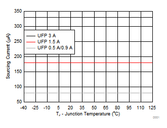
| ISRC | Sourcing current | VCHG = 0 V and VCHG_HI = 0 V 0 V ≤ VCCx ≤ 1.5 V |
75 | 80 | 85 | µA |
| VCHG = VAUX and VCHG_HI = 0 V 0 V ≤ VCCx ≤ 1.5 V |
170 | 180 | 190 | |||
| VCHG = VAUX and VCHG_HI = VAUX
0 V ≤ VCCx ≤ 2.45 V |
312 | 330 | 348 | |||
| UFP, POL, AUDIO, DEBUG | ||||||
| VOL | Output low voltage | ISNK_PIN = 1 mA | 250 | mV | ||
| IOFF | Off-state leakage | VPIN = 5.5 V | 1 | µA | ||
| EN, CHG, CHG_HI - LOGIC INPUTS | ||||||
| VTH | Rising threshold voltage | 0.925 | 1.15 | V | ||
| VTH | Falling threshold voltage | 0.65 | 0.875 | V | ||
| Hysteresis(2) | 50 | mV | ||||
| IIN | Input current | VEN = 0 V or 6.5 V | –0.5 | 0.5 | µA | |
| OVER TEMPERATURE SHUT DOWN | ||||||
| TTH_OTSD2 | Rising threshold temperature for device shutdown | 155 | °C | |||
| Hysteresis(2) | 20 | °C | ||||
| TTH_OTSD1 | Rising threshold temperature for OUT/ VCONN switch shutdown in current limit | 135 | °C | |||
| Hysteresis(2) | 20 | °C | ||||
| IN1 | ||||||
| VTH_UVLO_IN1 | Rising threshold voltage for UVLO | 3.9 | 4.1 | 4.3 | V | |
| Hysteresis(2) | 100 | mV | ||||
| II | Disabled supply current | VEN = 0 V, -40°C ≤ TJ ≤ 85°C | 1 | µA | ||
| Enabled supply current with CC lines open | -40°C ≤ TJ ≤ 85°C | 1 | µA | |||
| Enabled supply current with accessory or dangling electronically marked cable signature on CC lines | 2 | µA | ||||
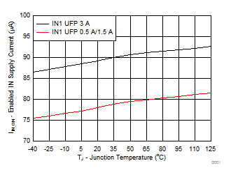
| Enabled supply current with UFP attached | VCHG = 0 V, or VCHG = VAUX and VCHG_HI = 0 V | 75 | 100 | µA | ||
| 85 | 110 | |||||
| IN2 | ||||||
| VTH_UVLO_IN2 | Rising threshold voltage for UVLO | 3.9 | 4.1 | 4.3 | V | |
| Hysteresis(2) | 100 | mV | ||||
| II | Disabled supply current | VEN = 0 V, -40°C ≤ TJ ≤ 85°C | 1 | µA | ||
| Enabled supply current with CC lines open | -40°C ≤ TJ ≤ 85°C | 1 | µA | |||
| II | Enabled supply current with accessory or dangling electronically marked cable signature on CC lines | 2 | µA | |||
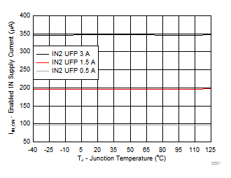
| II | Enabled supply current with UFP signature on CC lines (Includes IN current that provides the CC output current to the UFP Rd resistor) |
VCHG = 0 V, 0 V ≤ VCCx ≤ 1.5 V | 98 | 110 | µA | |
| VCHG = VIN and VCHG_HI = 0 V, 0 V ≤ VCCx ≤ 1.5 V | 198 | 215 | ||||
| 0 V ≤ VCCx ≤ 2.45 V | 348 | 373 | ||||
| AUX | ||||||
| VTH_UVLO_AUX | Rising threshold voltage for UVLO | 2.65 | 2.75 | 2.85 | V | |
| Hysteresis(2) | 100 | mV | ||||
| II | Disabled supply current | VEN = 0 V, -40°C ≤ TJ ≤ 85°C | 1 | µA | ||
| II | Enabled internal supply current with CC lines open | -40°C ≤ TJ ≤ 85°C | 0.7 | 3 | µA | |
| II | Enabled supply current with accessory or dangling active cable signature on CC lines | 140 | 185 | µA | ||
| II | Enabled supply current with UFP termination on CC lines and with either IN1 or IN2 in UVLO | VIN1 < VTH_UVLO_IN1 or VIN2 < VTH_UVLO_IN2 | 145 | 190 | µA | |
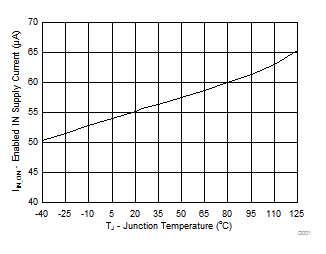
| II | Enabled supply current with UFP termination on CC lines | 55 | 82 | µA | ||
(1) Pulse-testing techniques maintain junction temperature close to ambient temperature; thermal effects must be taken into account separately.
(2) These parameters are provided for reference only and do not constitute part of TI’s published specifications for purposes of TI’s product warranty.
6.6 Switching Characteristics
–40°C ≤ TJ ≤ 125°C, 4.5 V ≤ VIN1 ≤ 6.5 V, 4.5 V ≤ VIN2 ≤ 5.5 V, 2.9 V ≤ VAUX ≤ 5.5 V; VEN = VCHG = VCHG_HI = VAUX, RREF = 100 kΩ. Typical values are at 25°C. All voltages are with respect to GND. IOUT and IOS defined positive out of the indicated pin (unless otherwise noted)| PARAMETER | TEST CONDITIONS | MIN | TYP | MAX | UNIT | |
|---|---|---|---|---|---|---|
| OUT - POWER SWITCH | ||||||
| tr | Output voltage rise time | VIN1 = 5 V, CL = 1 µF, RL = 100 Ω (measured from 10% to 90% of final value) | 1.2 | 1.8 | 2.5 | ms |
| tf | Output voltage fall time | 0.35 | 0.55 | 0.75 | ms | |
| ton | Output voltage turn-on time | VIN1 = 5 V, CL = 1 µF, RL = 100 Ω | 2.5 | 3.5 | 5 | ms |
| toff | Output voltage turn-off time | 2 | 3 | 4.5 | ms | |
| OUT - CURRENT LIMIT | ||||||
| tios | Current limit response time to short circuit | VIN1 - VOUT = 1 V, RL = 10 mΩ, see Figure 1 | 1.5 | 4 | µs | |
| FAULT | ||||||
| tDEGA | Asserting deglitch due to over current | 5.5 | 8.2 | 10.7 | ms | |
| tDEGA | Asserting deglitch due to over temperature in current limit(1) | 0 | ms | |||
| tDEGD | De-asserting deglitch | 5.5 | 8.2 | 10.7 | ms | |
| LD_DET | ||||||
| tDEGA | Asserting deglitch | 45 | 65 | 85 | ms | |
| tDEGD | De-asserting deglitch | 1.45 | 2.15 | 2.9 | s | |
| OUT - DISCHARGE | ||||||
| RDCHG discharge time | VOUT = 1 V, time ISNK_OUT > 1 mA after UFP signature removed from CC lines | 39 | 65 | 96 | ms | |
| CC1/CC2 - VCONN POWER SWITCH | ||||||
| tr | Output voltage rise time | VIN2 = 5 V, CL = 1 µF, RL = 100 Ω (measured from 10% to 90% of final value) | 0.15 | 0.25 | 0.35 | ms |
| tf | Output voltage fall time | 0.18 | 0.22 | 0.26 | ms | |
| ton | Output voltage turn-on time | VIN2 = 5 V, CL = 1 µF, RL = 100 Ω | 1 | 1.5 | 2 | ms |
| toff | Output voltage turn-off time | 0.3 | 0.4 | 0.55 | ms | |
| CC1/CC2 - VCONN POWER SWITCH - CURRENT LIMIT | ||||||
| tres | Current limit response time to short circuit | VIN2 – VCONN = 1 V, R = 10 mΩ, see Figure 1 | 1 | 3 | µs | |
| UFP, POL, AUDIO, DEBUG | ||||||
| tDEGR | Asserting deglitch | 100 | 150 | 200 | ms | |
| tDEGF | De-asserting deglitch | 7.9 | 12.5 | 17.7 | ms | |
(1) These parameters are provided for reference only and do not constitute part of TI’s published specifications for purposes of TI’s product warranty.
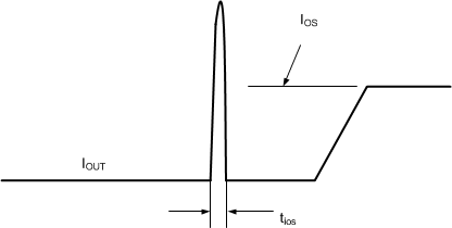 Figure 1. Output Short Circuit Parameter Diagram
6.7 Typical Characteristics
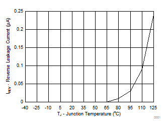
| Device = Disabled; (VOUT-VIN) =6.5V | ||
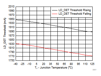
| VAUX = 5 V |
