ZHCSK24D July 2019 – July 2021 TPS25832-Q1 , TPS25833-Q1
PRODUCTION DATA
- 1 特性
- 2 应用
- 3 说明
- 4 Revision History
- 5 说明(续)
- 6 Device Comparison Table
- 7 Pin Configuration and Functions
- 8 Specifications
- 9 Parameter Measurement Information
-
10Detailed Description
- 10.1 Overview
- 10.2 Functional Block Diagram
- 10.3
Feature Description
- 10.3.1 Buck Regulator
- 10.3.2 Enable/UVLO and Start-up
- 10.3.3 RT/SYNC
- 10.3.4 Spread-Spectrum Operation
- 10.3.5 VCC, VCC_UVLO
- 10.3.6 Minimum ON-time, Minimum OFF-time
- 10.3.7 Internal Compensation
- 10.3.8 Bootstrap Voltage (BOOT)
- 10.3.9 RSNS, RSET, RILIMIT, and RIMON
- 10.3.10 Overcurrent and Short Circuit Protection
- 10.3.11 IEC and Overvoltage Protection
- 10.3.12 Cable Compensation
- 10.3.13 USB Port Control
- 10.3.14 FAULT Response
- 10.3.15 USB Specification Overview
- 10.3.16 USB Type-C® Basics
- 10.3.17 Device Power Pins (IN, CSN/OUT, and PGND)
- 10.3.18 Thermal Shutdown
- 10.3.19 Power Wake
- 10.3.20 Thermal Sensing with NTC (TPS25833-Q1)
- 10.4
Device Functional Modes
- 10.4.1 Shutdown Mode
- 10.4.2 Standby Mode
- 10.4.3 Active Mode
- 10.4.4 Device Truth Table (TT)
- 10.4.5 USB Port Operating Modes
- 10.4.6 High-Bandwidth Data-Line Switches (TPS25832-Q1 Only)
-
11Application and Implementation
- 11.1 Application Information
- 11.2
Typical Application
- 11.2.1 Design Requirements
- 11.2.2
Detailed Design Procedure
- 11.2.2.1 Output Voltage
- 11.2.2.2 Switching Frequency
- 11.2.2.3 Inductor Selection
- 11.2.2.4 Output Capacitor Selection
- 11.2.2.5 Input Capacitor Selection
- 11.2.2.6 Bootstrap Capacitor Selection
- 11.2.2.7 VCC Capacitor Selection
- 11.2.2.8 Enable and Under Voltage Lockout Set-Point
- 11.2.2.9 Current Limit Set-Point
- 11.2.2.10 Cable Compensation Set-Point
- 11.2.2.11 LD_DET, POL, and FAULT Resistor Selection
- 11.2.3 Application Curves
- 12Power Supply Recommendations
- 13Layout
- 14Device and Documentation Support
- 15Mechanical, Packaging, and Orderable Information
10.3.2 Enable/UVLO and Start-up
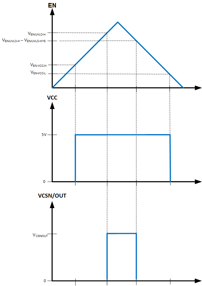
The voltage on the EN/UVLO pin controls the ON or OFF operation of TPS2583x-Q1. An EN/UVLO pin voltage higher than VEN/UVLO-VOUT-H is required to start the internal regulator and begin monitoring the CCn lines for a valid Type-C connection. The internal USB monitoring circuitry is on when VIN is within the operation range and the EN/UVLO threshold is cleared; however, the buck regulator does not begin operation until a valid USB Type-C detection has been made. This feature ensures the "cold socket" (0 V) USB Type-C VBUS requirement is met. The EN/UVLO pin is an input and can not be left open or floating. The simplest way to enable the operation of the TPS2583x-Q1 is to connect the EN to VIN. This allows self-start-up of the TPS2583x-Q1 when VIN is within the operation range.
 Figure 10-2 Precision Enable Behavior
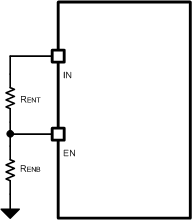
Many applications will benefit from the employment of an enable divider RENT and RENB (Figure 10-3) to establish a precision system UVLO level for the TPS2583x-Q1. The system UVLO can be used for sequencing, ensuring reliable operation, or supply protection, such as a battery discharge level. To ensure the USB port VBUS is within the 5-V operating range as required for USB compliance (for the latest USB specifications and requirements, refer to USB.org), TI suggests that the RENT and RENB resistors be chosen such that the TPS2583x-Q1 enables when VIN is approximately 6 V. Considering the drop out voltage of the buck regulator and IR loses in the system, 6 V provides adequate margin to maintain VBUS within USB specifications. If system requirements such as a warm crank (start) automotive scenario require operation with VIN < 6 V, the values of RENT and RENB can be calculated assuming a lower VIN. An external logic signal can also be used to drive EN/UVLO input when a microcontroller is present and it is desirable to enable or disable the USB port remotely for other reasons.
 Figure 10-3 System UVLO by Enable Divider
UVLO configuration using external resistors is governed by the following equations:


Example:
VIN(ON) = 6 V (user choice)
RENB = 5 kΩ (user choice)
RENT = [(VIN(ON) / VEN/UVLO_H) – 1] × RENB= 19.6 kΩ. Choose standard 20 kΩ.
Therefore VIN(OFF) = 6 V × [1 - (0.09 V / 1.2 V)] = 5.55 V
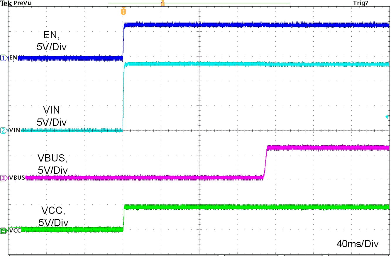
A typical start-up waveform is shown in Figure 10-4, indicating typical timings when Rd connected to CC line. The rise time of DCDC VBUS voltage is about 5 ms.
 Figure 10-4 Typical Start-up Behavior, VIN = 13.5 V, CC1 = Rd, RIMON = 12.6 kΩ
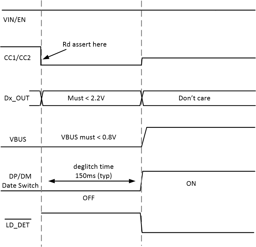
For TPS25832-Q1, the pin voltage must meet the requirement below during 150-ms (typ) Rd assert deglitch time, see Figure 10-5:
- VBUS < 0.8 V (typical), per Type-C requirement
- VDx_OUT < 2.2 V (typical)
- VDx_IN < 1.5 V (typical)
After the TPS25832-Q1 Rd assert deglitch time, no additional requirement on these pins. In real application, LD_DET pin can be used to configure the timing sequence.
 Figure 10-5 TPS25832-Q1 Pin Voltage
Requirement During Rd Assert