ZHCSK24D July 2019 – July 2021 TPS25832-Q1 , TPS25833-Q1
PRODUCTION DATA
- 1 特性
- 2 应用
- 3 说明
- 4 Revision History
- 5 说明(续)
- 6 Device Comparison Table
- 7 Pin Configuration and Functions
- 8 Specifications
- 9 Parameter Measurement Information
-
10Detailed Description
- 10.1 Overview
- 10.2 Functional Block Diagram
- 10.3
Feature Description
- 10.3.1 Buck Regulator
- 10.3.2 Enable/UVLO and Start-up
- 10.3.3 RT/SYNC
- 10.3.4 Spread-Spectrum Operation
- 10.3.5 VCC, VCC_UVLO
- 10.3.6 Minimum ON-time, Minimum OFF-time
- 10.3.7 Internal Compensation
- 10.3.8 Bootstrap Voltage (BOOT)
- 10.3.9 RSNS, RSET, RILIMIT, and RIMON
- 10.3.10 Overcurrent and Short Circuit Protection
- 10.3.11 IEC and Overvoltage Protection
- 10.3.12 Cable Compensation
- 10.3.13 USB Port Control
- 10.3.14 FAULT Response
- 10.3.15 USB Specification Overview
- 10.3.16 USB Type-C® Basics
- 10.3.17 Device Power Pins (IN, CSN/OUT, and PGND)
- 10.3.18 Thermal Shutdown
- 10.3.19 Power Wake
- 10.3.20 Thermal Sensing with NTC (TPS25833-Q1)
- 10.4
Device Functional Modes
- 10.4.1 Shutdown Mode
- 10.4.2 Standby Mode
- 10.4.3 Active Mode
- 10.4.4 Device Truth Table (TT)
- 10.4.5 USB Port Operating Modes
- 10.4.6 High-Bandwidth Data-Line Switches (TPS25832-Q1 Only)
-
11Application and Implementation
- 11.1 Application Information
- 11.2
Typical Application
- 11.2.1 Design Requirements
- 11.2.2
Detailed Design Procedure
- 11.2.2.1 Output Voltage
- 11.2.2.2 Switching Frequency
- 11.2.2.3 Inductor Selection
- 11.2.2.4 Output Capacitor Selection
- 11.2.2.5 Input Capacitor Selection
- 11.2.2.6 Bootstrap Capacitor Selection
- 11.2.2.7 VCC Capacitor Selection
- 11.2.2.8 Enable and Under Voltage Lockout Set-Point
- 11.2.2.9 Current Limit Set-Point
- 11.2.2.10 Cable Compensation Set-Point
- 11.2.2.11 LD_DET, POL, and FAULT Resistor Selection
- 11.2.3 Application Curves
- 12Power Supply Recommendations
- 13Layout
- 14Device and Documentation Support
- 15Mechanical, Packaging, and Orderable Information
10.3.5 VCC, VCC_UVLO
The TPS2583x-Q1 integrates an internal LDO to generate VCC for control circuitry and MOSFET drivers. The nominal voltage for VCC is 5 V. The VCC pin is the output of an LDO and must be properly bypassed. A high quality ceramic capacitor with a value of 2.2 µF to 4.7 µF, 10 V or higher rated voltage should be placed as close as possible to VCC and grounded to the PGND ground pin. The VCC output pin should not be loaded with more than 5 mA, or shorted to ground during operation. Shorting VCC to ground during operation may cause damage to the TPS2583x-Q1.
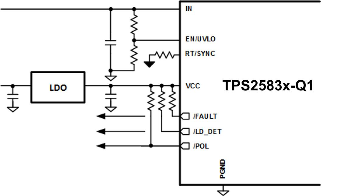
In applications where VCONN support is required, the VCC pin can be over-driven with an external 5-V LDO capable of sourcing at least 300 mA. In this operating mode the external LDO is the source for the buck low-side switch gate drive as well as power to the internal VCONN mux.
Note if using external 5-V LDO for VCONN power, the timing sequence below must be required. External VCONN power can not be enabled before the TPS2583x-Q1 is enabled, external VCONN must be disabled before the TPS2583x-Q1 is disabled. In real application, customer can tie the EN of external 5-V LDO and EN of TPS2583x-Q1 together to meet the timing requirement.
 Figure 10-14 VCONN Source Using External LDO