ZHCSK24D July 2019 – July 2021 TPS25832-Q1 , TPS25833-Q1
PRODUCTION DATA
- 1 特性
- 2 应用
- 3 说明
- 4 Revision History
- 5 说明(续)
- 6 Device Comparison Table
- 7 Pin Configuration and Functions
- 8 Specifications
- 9 Parameter Measurement Information
-
10Detailed Description
- 10.1 Overview
- 10.2 Functional Block Diagram
- 10.3
Feature Description
- 10.3.1 Buck Regulator
- 10.3.2 Enable/UVLO and Start-up
- 10.3.3 RT/SYNC
- 10.3.4 Spread-Spectrum Operation
- 10.3.5 VCC, VCC_UVLO
- 10.3.6 Minimum ON-time, Minimum OFF-time
- 10.3.7 Internal Compensation
- 10.3.8 Bootstrap Voltage (BOOT)
- 10.3.9 RSNS, RSET, RILIMIT, and RIMON
- 10.3.10 Overcurrent and Short Circuit Protection
- 10.3.11 IEC and Overvoltage Protection
- 10.3.12 Cable Compensation
- 10.3.13 USB Port Control
- 10.3.14 FAULT Response
- 10.3.15 USB Specification Overview
- 10.3.16 USB Type-C® Basics
- 10.3.17 Device Power Pins (IN, CSN/OUT, and PGND)
- 10.3.18 Thermal Shutdown
- 10.3.19 Power Wake
- 10.3.20 Thermal Sensing with NTC (TPS25833-Q1)
- 10.4
Device Functional Modes
- 10.4.1 Shutdown Mode
- 10.4.2 Standby Mode
- 10.4.3 Active Mode
- 10.4.4 Device Truth Table (TT)
- 10.4.5 USB Port Operating Modes
- 10.4.6 High-Bandwidth Data-Line Switches (TPS25832-Q1 Only)
-
11Application and Implementation
- 11.1 Application Information
- 11.2
Typical Application
- 11.2.1 Design Requirements
- 11.2.2
Detailed Design Procedure
- 11.2.2.1 Output Voltage
- 11.2.2.2 Switching Frequency
- 11.2.2.3 Inductor Selection
- 11.2.2.4 Output Capacitor Selection
- 11.2.2.5 Input Capacitor Selection
- 11.2.2.6 Bootstrap Capacitor Selection
- 11.2.2.7 VCC Capacitor Selection
- 11.2.2.8 Enable and Under Voltage Lockout Set-Point
- 11.2.2.9 Current Limit Set-Point
- 11.2.2.10 Cable Compensation Set-Point
- 11.2.2.11 LD_DET, POL, and FAULT Resistor Selection
- 11.2.3 Application Curves
- 12Power Supply Recommendations
- 13Layout
- 14Device and Documentation Support
- 15Mechanical, Packaging, and Orderable Information
10.3.20 Thermal Sensing with NTC (TPS25833-Q1)
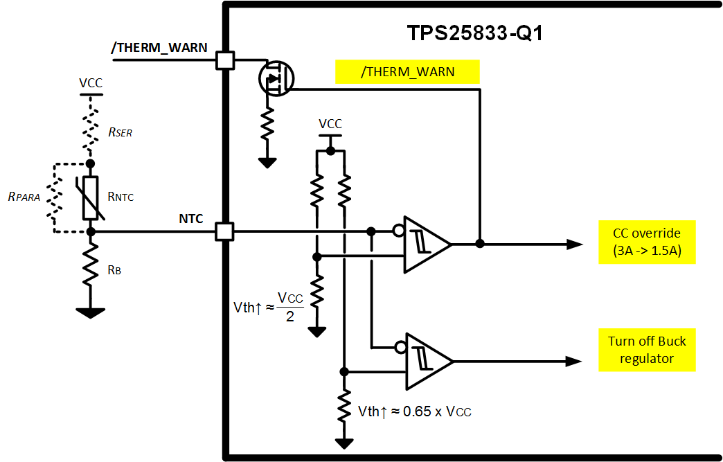
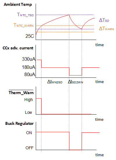
The NTC input pin allows for user programmable thermal protection. See Electrical Characteristics for NTC pin thresholds. The NTC input pin threshold is ratiometric with VCC. The external resistor divider setting VNTC must be connected to the TPS25833-Q1 VCC pin to achieve accurate results. See Figure 10-28 and Figure 10-29. When VNTC = 0.5 × VCC (approximately 2.5 V typically), the TPS25833-Q1 performs two actions:
- If operating with 3-A Type-C advertisement, the CC1 and CC2 pin automatically reduces advertisement to the 1.5-A level.
- The THERM_WARN flag is asserted to provide an indication of the overtemperature condition. FAULT is NOT asserted at this time.
 Figure 10-28 NTC Input Pin
 Figure 10-29 TPS25833-Q1 Behavior when Trigger NTC Threshold
If the overtemprature condition persists causing VNTC = VCC × 0.65 (3.25-V typical), the TPS25833-Q1 turns off the buck regulator and pulls the LS_GD pin low. The THERM_WARN flag remains asserted; however, the FAULT pin is NOT asserted for this condition.
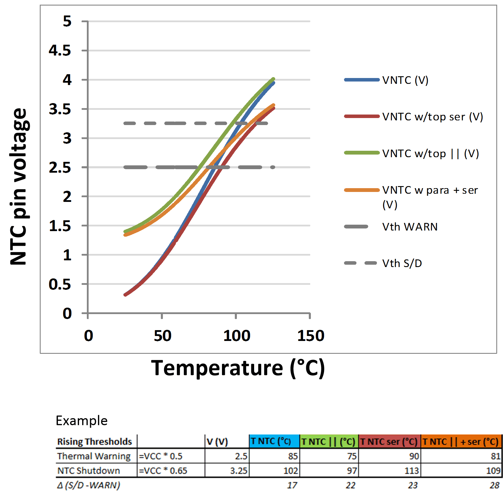
Tuning the VNTC threshold levels of VWARN_HIGH and VSD_HIGH is achieved by adding RSER, RPARA, or both RSER and RPARA in conjunction with RNTC. Figure 10-30 is an example illustrating how to set the THERM_WARN threshold between 75°C and 90°C with a ΔT between THERM_WARN assertion and device shutdown of 17°C to 28°C. Consult the chosen NTC manufacturer's specification for the value of β. It may take some iteration to establish the desired warning and shutdown thresholds.
Below is NTC spec and resistor value used in Figure 10-30 example.
- R0 = 470 kΩ. β = 4750. RNTC=R0 × exp β × (1/T-1/T0)
- RPARA = 100 kΩ.
- RSER = 5 kΩ.
- RB = RNTC(at T_ THERM_WARN) = 32 kΩ
 Figure 10-30 VNTC Threshold Examples
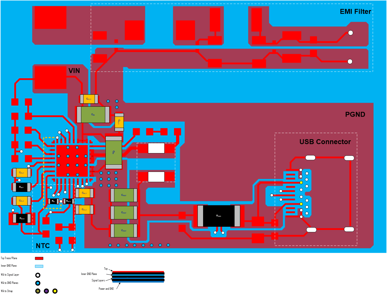
The NTC resistor should be placed near the hottest point on the PCB. In most cases, this will be close to the SW node of the TPS25833-Q1, near the buck inductor, RSNS sense resistor and external MOSFETs (if used).
 Figure 10-31 NTC Placement Example