ZHCSK24D July 2019 – July 2021 TPS25832-Q1 , TPS25833-Q1
PRODUCTION DATA
- 1 特性
- 2 应用
- 3 说明
- 4 Revision History
- 5 说明(续)
- 6 Device Comparison Table
- 7 Pin Configuration and Functions
- 8 Specifications
- 9 Parameter Measurement Information
-
10Detailed Description
- 10.1 Overview
- 10.2 Functional Block Diagram
- 10.3
Feature Description
- 10.3.1 Buck Regulator
- 10.3.2 Enable/UVLO and Start-up
- 10.3.3 RT/SYNC
- 10.3.4 Spread-Spectrum Operation
- 10.3.5 VCC, VCC_UVLO
- 10.3.6 Minimum ON-time, Minimum OFF-time
- 10.3.7 Internal Compensation
- 10.3.8 Bootstrap Voltage (BOOT)
- 10.3.9 RSNS, RSET, RILIMIT, and RIMON
- 10.3.10 Overcurrent and Short Circuit Protection
- 10.3.11 IEC and Overvoltage Protection
- 10.3.12 Cable Compensation
- 10.3.13 USB Port Control
- 10.3.14 FAULT Response
- 10.3.15 USB Specification Overview
- 10.3.16 USB Type-C® Basics
- 10.3.17 Device Power Pins (IN, CSN/OUT, and PGND)
- 10.3.18 Thermal Shutdown
- 10.3.19 Power Wake
- 10.3.20 Thermal Sensing with NTC (TPS25833-Q1)
- 10.4
Device Functional Modes
- 10.4.1 Shutdown Mode
- 10.4.2 Standby Mode
- 10.4.3 Active Mode
- 10.4.4 Device Truth Table (TT)
- 10.4.5 USB Port Operating Modes
- 10.4.6 High-Bandwidth Data-Line Switches (TPS25832-Q1 Only)
-
11Application and Implementation
- 11.1 Application Information
- 11.2
Typical Application
- 11.2.1 Design Requirements
- 11.2.2
Detailed Design Procedure
- 11.2.2.1 Output Voltage
- 11.2.2.2 Switching Frequency
- 11.2.2.3 Inductor Selection
- 11.2.2.4 Output Capacitor Selection
- 11.2.2.5 Input Capacitor Selection
- 11.2.2.6 Bootstrap Capacitor Selection
- 11.2.2.7 VCC Capacitor Selection
- 11.2.2.8 Enable and Under Voltage Lockout Set-Point
- 11.2.2.9 Current Limit Set-Point
- 11.2.2.10 Cable Compensation Set-Point
- 11.2.2.11 LD_DET, POL, and FAULT Resistor Selection
- 11.2.3 Application Curves
- 12Power Supply Recommendations
- 13Layout
- 14Device and Documentation Support
- 15Mechanical, Packaging, and Orderable Information
10.3.16.2 Detecting a Connection
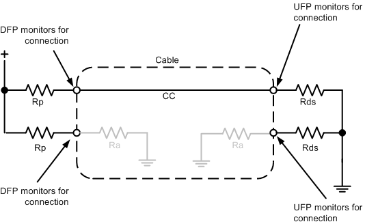
DFPs and DRPs fulfill the role of detecting a valid connection over USB Type-C. Figure 10-25 shows a DFP to UFP connection made with Type C cable. As shown in Figure 10-25, the detection concept is based on being able to detect terminations in the product which has been attached. A pull-up and pull-down termination model is used. A pull-up termination can be replaced by a current source. TPS2583x-Q1 devices use current sources in lieu of RP as allowed by the Type-C specification.
- In the DFP-UFP connection the DFP monitors both CC pins for a voltage lower than the unterminated voltage.
- An UFP advertises Rd on both its CC pins (CC1 and CC2).
- A powered cable advertises Ra on only one of CC pins of the plug. Ra is used to inform the source to apply VCONN.
- An analog audio device advertises Ra on both CC pins of the plug, which identifies it as an analog audio device. VCONN is not applied on either CC pin in this case.
 Figure 10-25 DFP-UFP Connection