ZHCSK92E September 2019 – March 2022 TPS25840-Q1 , TPS25842-Q1
PRODUCTION DATA
- 1 特性
- 2 应用
- 3 说明
- 4 Revision History
- 5 说明(续)
- 6 Device Comparison Table
- 7 Pin Configuration and Functions
- 8 Specifications
- 9 Parameter Measurement Information
-
10Detailed Description
- 10.1 Overview
- 10.2 Functional Block Diagram
- 10.3
Feature Description
- 10.3.1 Buck Regulator
- 10.3.2 Enable/UVLO
- 10.3.3 Switching Frequency and Synchronization (RT/SYNC)
- 10.3.4 Spread-Spectrum Operation
- 10.3.5 VCC, VCC_UVLO
- 10.3.6 Minimum ON-time, Minimum OFF-time
- 10.3.7 Internal Compensation
- 10.3.8 Bootstrap Voltage (BOOT)
- 10.3.9 RSNS, RSET, RILIMIT and RIMON
- 10.3.10 Overcurrent and Short Circuit Protection
- 10.3.11 Overvoltage, IEC and Short-to-Battery Protection
- 10.3.12 Cable Compensation
- 10.3.13 USB Port Control
- 10.3.14 FAULT Response
- 10.3.15 USB Specification Overview
- 10.3.16 Device Power Pins (IN, CSN/OUT, and PGND)
- 10.3.17 Thermal Shutdown
- 10.4 Device Functional Modes
-
11Application and Implementation
- 11.1 Application Information
- 11.2
Typical Application
- 11.2.1 Design Requirements
- 11.2.2
Detailed Design Procedure
- 11.2.2.1 Output Voltage
- 11.2.2.2 Switching Frequency
- 11.2.2.3 Inductor Selection
- 11.2.2.4 Output Capacitor Selection
- 11.2.2.5 Input Capacitor Selection
- 11.2.2.6 Bootstrap Capacitor Selection
- 11.2.2.7 VCC Capacitor Selection
- 11.2.2.8 Enable and Under Voltage Lockout Set-Point
- 11.2.2.9 Current Limit Set-Point
- 11.2.2.10 Cable Compensation Set-Point
- 11.2.2.11 FAULT Resistor Selection
- 11.2.3 Application Curves
- 12Power Supply Recommendations
- 13Layout
- 14Device and Documentation Support
- 15Mechanical, Packaging, and Orderable Information
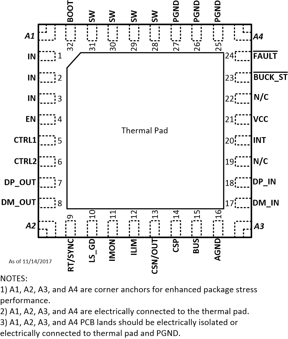
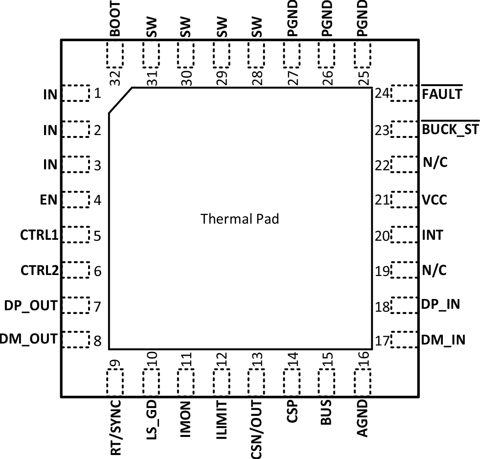
7 Pin Configuration and Functions
Table 7-1 Pin Functions
| PIN | TYPE(3) | I/O | DESCRIPTION | |
|---|---|---|---|---|
| NAME | NO. | |||
| AGND | 16 | G | - | Analog ground terminal. Ground reference for internal references and logic. All electrical parameters are measured with respect to this pin. Connect to system ground on PCB. |
| BOOT | 32 | P | Boot-strap capacitor connection for HS FET driver. Connect a high quality 100-nF capacitor from this pin to the SW pin. | |
| BUS | 15 | A | I | VBUS discharge input. Connect to VBUS on USB Connector. |
| CSN/OUT | 13 | P | I | Negative input of current sense amplifier, also buck output for internal voltage regulation. |
| CSP | 14 | P | I | Positive input of current sense amplifier. |
| CTRL1 | 5 | A | I | Logic-level control inputs for device and system configuration (see Table 10-6). |
| CTRL2 | 6 | A | I | Logic-level control inputs for device and system configuration (see Table 10-6). |
| DM_IN | 17 | A | DM data line. Connect to USB connector. | |
| DM_OUT | 8 | A | DM data line. Connect to USB host controller. | |
| DP_IN | 18 | A | DP data line. Connect to USB connector. | |
| DP_OUT | 7 | A | DP data line. Connect to USB host controller. | |
| EN/UVLO | 4 | A | Enable pin. Do not float. High = on, Low = off. Can be tied to VIN. Precision enable input allows adjustable UVLO by external resistor divider. | |
| FAULT | 24 | A | O | Active LOW open-drain output. Asserted during fault conditions (see Table 10-4). TI recommends series about 1-k ohm damping resistor for better signal quality. |
| ILIMIT | 12 | A | External resistor used to set the current-limit threshold (see Table 10-2). | |
| IMON | 11 | A | External resistor used to set the max cable comp voltage at full load current. | |
| IN | 1, 2, 3 | P | I | Input Supply to regulator. Connect high-quality bypass capacitors directly to this pin and PGND. |
| BUCK_ST | 23 | A | O | Active Low open-drain output. After BUCK_ST assert, the Buck converter begins to start up. At the same time, DP and DM data switch turn on accordingly. |
| LS_GD | 10 | A | External NMOS gate driver. If TPS2584x-Q1 configured under average current limit mode, LS_GD pin must be pulled up through a 2.2-kΩ resistor (see Current Limit Sensing using RILIMIT). | |
| PGND | 25, 26, 27 | G | Power ground terminal. Connect to system ground and AGND. Connect to bypass capacitor with short wide traces. | |
| N/C | 19, 22 | - | Make no electrical connection. | |
| RT/SYNC | 9 | A | Resistor Timing or External Clock input. An internal amplifier holds this terminal at a fixed voltage when using an external resistor to ground to set the switching frequency. If the terminal is pulled above the PLL upper threshold, a mode change occurs and the terminal becomes a synchronization input. The internal amplifier is disabled and the terminal is a high impedance clock input to the internal PLL. If clocking edges stop, the internal amplifier is re-enabled and the operating mode returns to resistor frequency programming. | |
| SW | 28, 29, 30, 31 | P | Switching output of the regulator. Internally connected to source of the HS FET and drain of the LS FET. Connect to power inductor. | |
| INT | 20 | A | For internal circuit, must connect a 5.1-K resistor to AGND. | |
| VCC | 21 | P | Output of internal bias supply. Used as supply to internal control circuits. Connect a high quality 2.2-µF capacitor from this pin to GND. | |
(1) For package drawing please refer to RHB0032R at the end of the data sheet.
(2) For package drawing please refer
to RHB0032AA at the end of the data sheet.
(3) A = Analog, P = Power, G = Ground.

