ZHCSOR1 August 2021 TPS25860-Q1 , TPS25862-Q1
PRODUCTION DATA
- 1 特性
- 2 应用
- 3 说明
- 4 Revision History
- 5 说明(续)
- 6 Device Comparison Table
- 7 Pin Configuration and Functions
- 8 Specifications
- 9 Parameter Measurement Information
-
10Detailed Description
- 10.1 Overview
- 10.2 Functional Block Diagram
- 10.3
Feature Description
- 10.3.1 Power-Down or Undervoltage Lockout
- 10.3.2 Input Overvoltage Protection (OVP) - Continuously Monitored
- 10.3.3 Buck Converter
- 10.3.4 FREQ/SYNC
- 10.3.5 Bootstrap Voltage (BOOT)
- 10.3.6 Minimum ON-Time, Minimum OFF-Time
- 10.3.7 Internal Compensation
- 10.3.8 Selectable Output Voltage (VSET)
- 10.3.9 Current Limit and Short Circuit Protection
- 10.3.10 Cable Compensation
- 10.3.11 Thermal Management with Temperature Sensing (TS) and OTSD
- 10.3.12 Thermal Shutdown
- 10.3.13 USB Enable On/Off Control (TPS25862-Q1)
- 10.3.14 FAULT Indication
- 10.3.15 USB Specification Overview
- 10.3.16 USB Type-C® Basics
- 10.3.17 USB Port Operating Modes
- 10.4 Device Functional Modes
-
11Application and Implementation
- 11.1 Application Information
- 11.2
Typical Applications
- 11.2.1 Design Requirements
- 11.2.2
Detailed Design Procedure
- 11.2.2.1 Output Voltage Setting
- 11.2.2.2 Switching Frequency
- 11.2.2.3 Inductor Selection
- 11.2.2.4 Output Capacitor Selection
- 11.2.2.5 Input Capacitor Selection
- 11.2.2.6 Bootstrap Capacitor Selection
- 11.2.2.7 Undervoltage Lockout Set-Point
- 11.2.2.8 Cable Compensation Set-Point
- 11.2.2.9 FAULT Resistor Selection
- 11.2.3 Application Curves
- 12Power Supply Recommendations
- 13Layout
- 14Device and Documentation Support
- 15Mechanical, Packaging, and Orderable Information
10.3.3 Buck Converter
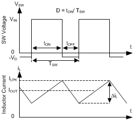
The following operating description of the TPS2586x-Q1 refers to the Functional Block Diagram. The TPS2586x-Q1 integrates a monolithic, synchronous, rectified, step-down, switch-mode converter with internal power MOSFETs and USB current-limit switches with charging ports auto-detection. The TPS2586x-Q1 offers a compact and high efficiency solution with excellent load and line regulation over a wide input supply range. The TPS2586x-Q1 supplies a regulated output voltage by turning on the high-side (HS) and low-side (LS) NMOS switches with controlled duty cycle. During high-side switch ON time, the SW pin voltage swings up to approximately VIN. The inductor current iL increases with linear slope (VIN – VOUT ) / L. When the HS switch is turned off by the control logic, the LS switch is turned on after an anti-shoot-through dead time. Inductor current discharges through the LS switch with a slope of –VOUT / L. The control parameter of a buck converter is defined as Duty Cycle D = tON / TSW, where tON is the high-side switch ON time and TSW is the switching period, shown in Figure 10-2. The regulator control loop maintains a constant output voltage by adjusting the duty cycle D. In an ideal buck converter, where losses are ignored, D is proportional to the output voltage and inversely proportional to the input voltage: D = VOUT / VIN.
 Figure 10-2 SW Node and Inductor Current Waveforms in Continuous Conduction Mode (CCM)
The TPS2586x-Q1 operates in a fixed-frequency, peak-current-mode control to regulate the output voltage. A voltage feedback loop is used to get accurate DC voltage regulation by adjusting the peak current command based on voltage offset. The peak inductor current is sensed from the high-side switch and compared to the peak current threshold to control the ON time of the high-side switch. The voltage feedback loop is internally compensated, which allows for fewer external components, making it easy to design, and provides stable operation with a reasonable combination of output capacitors. The TPS2586x-Q1 operates in FPWM mode for low output voltage ripple, tight output voltage regulation, and constant switching frequency.
The TPS2586x-Q1 also has variants to support PFM mode. In PFM mode, the high-side FET is turned on in a burst of one or more cycles to provide energy to the load. The frequency of these bursts is adjusted to regulate the output, while diode emulation is used to maximize efficiency. This mode provides high light-load efficiency by reducing the amount of input supply current required to regulate the output voltage at small loads. A small increase in the output voltage occurs in PFM. This mode trades off very good light load efficiency for larger output voltage ripple and variable switching frequency.