ZHCSMS4B November   2020  – September 2021 TPS25864-Q1 , TPS25865-Q1

PRODUCTION DATA  

  1. 特性
  2. 应用
  3. 说明
  4. Revision History
  5. 说明(续)
  6. Device Comparison Table
  7. Pin Configuration and Functions
  8. Specifications
    1. 8.1 Absolute Maximum Ratings
    2. 8.2 ESD Ratings
    3. 8.3 Recommended Operating Conditions
    4. 8.4 Thermal Information
    5. 8.5 Electrical Characteristics
    6. 8.6 Timing Requirements
    7. 8.7 Switching Characteristics
    8. 8.8 Typical Characteristics
  9. Parameter Measurement Information
  10. 10Detailed Description
    1. 10.1 Overview
    2. 10.2 Functional Block Diagram
    3. 10.3 Feature Description
      1. 10.3.1  Power-Down or Undervoltage Lockout
      2. 10.3.2  Input Overvoltage Protection (OVP) - Continuously Monitored
      3. 10.3.3  Buck Converter
      4. 10.3.4  FREQ/SYNC
      5. 10.3.5  Bootstrap Voltage (BOOT)
      6. 10.3.6  Minimum ON-Time, Minimum OFF-Time
      7. 10.3.7  Internal Compensation
      8. 10.3.8  Selectable Output Voltage (VSET)
      9. 10.3.9  Current Limit and Short Circuit Protection
        1. 10.3.9.1 USB Switch Current Limit
        2. 10.3.9.2 Interlocking for Two-Level USB Switch Current Limit
        3. 10.3.9.3 Cycle-by-Cycle Buck Current Limit
        4. 10.3.9.4 OUT Current Limit
      10. 10.3.10 Cable Compensation
      11. 10.3.11 Thermal Management With Temperature Sensing (TS) and OTSD
      12. 10.3.12 Thermal Shutdown
      13. 10.3.13 USB Specification Overview
      14. 10.3.14 USB Port Operating Modes
        1. 10.3.14.1 Dedicated Charging Port (DCP) Mode
          1. 10.3.14.1.1 DCP BC1.2 and YD/T 1591-2009
          2. 10.3.14.1.2 DCP Divider-Charging Scheme
          3. 10.3.14.1.3 DCP 1.2-V Charging Scheme
        2. 10.3.14.2 DCP Auto Mode
    4. 10.4 Device Functional Modes
      1. 10.4.1 Shutdown Mode
      2. 10.4.2 Active Mode
  11. 11Application and Implementation
    1. 11.1 Application Information
    2. 11.2 Typical Applications
      1. 11.2.1 Design Requirements
      2. 11.2.2 Detailed Design Procedure
        1. 11.2.2.1 Output Voltage Setting
        2. 11.2.2.2 Switching Frequency
        3. 11.2.2.3 Inductor Selection
        4. 11.2.2.4 Output Capacitor Selection
        5. 11.2.2.5 Input Capacitor Selection
        6. 11.2.2.6 Bootstrap Capacitor Selection
        7. 11.2.2.7 Undervoltage Lockout Set-Point
        8. 11.2.2.8 Cable Compensation Set-Point
      3. 11.2.3 Application Curves
  12. 12Power Supply Recommendations
  13. 13Layout
    1. 13.1 Layout Guidelines
    2. 13.2 Layout Example
    3. 13.3 Ground Plane and Thermal Considerations
  14. 14Device and Documentation Support
    1. 14.1 接收文档更新通知
    2. 14.2 支持资源
    3. 14.3 Trademarks
    4. 14.4 Electrostatic Discharge Caution
    5. 14.5 术语表
  15. 15Mechanical, Packaging, and Orderable Information

封装选项

机械数据 (封装 | 引脚)
散热焊盘机械数据 (封装 | 引脚)
订购信息
DCP 1.2-V Charging Scheme

The DCP 1.2-V charging scheme is used by some hand-held devices to enable fast charging at 2 A. The TPS2586x-Q1 device supports this scheme in DCP-auto state before the device enters BC1.2 shorted mode. To simulate this charging scheme, the D+ and D– lines are shorted and pulled up to 1.2 V for a fixed duration. Then the device moves to DCP shorted mode as defined in the BC1.2 specification and as shown in Figure 10-13.
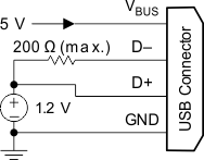
GUID-EF5077CD-766F-479C-BFC5-B40C18B21EBD-low.gifFigure 10-13 1.2-V Mode