ZHCSOR0 August 2021 TPS25868-Q1 , TPS25869-Q1
PRODUCTION DATA
- 1 特性
- 2 应用
- 3 说明
- 4 Revision History
- 5 说明(续)
- 6 Device Comparison Table
- 7 Pin Configuration and Functions
- 8 Specifications
- 9 Parameter Measurement Information
-
10Detailed Description
- 10.1 Overview
- 10.2 Functional Block Diagram
- 10.3
Feature Description
- 10.3.1 Power-Down or Undervoltage Lockout
- 10.3.2 Input Overvoltage Protection (OVP) - Continuously Monitored
- 10.3.3 Buck Converter
- 10.3.4 FREQ/SYNC
- 10.3.5 Bootstrap Voltage (BOOT)
- 10.3.6 Minimum ON-Time, Minimum OFF-Time
- 10.3.7 Internal Compensation
- 10.3.8 Selectable Output Voltage (VSET)
- 10.3.9 Current Limit and Short Circuit Protection
- 10.3.10 Cable Compensation
- 10.3.11 Thermal Management with Temperature Sensing (TS) and OTSD
- 10.3.12 Thermal Shutdown
- 10.3.13 USB Enable On/Off Control (TPS25869-Q1)
- 10.3.14 FAULT Indication
- 10.3.15 USB Specification Overview
- 10.3.16 USB Type-C® Basics
- 10.3.17 USB Port Operating Modes
- 10.4 Device Functional Modes
-
11Application and Implementation
- 11.1 Application Information
- 11.2
Typical Applications
- 11.2.1 Design Requirements
- 11.2.2
Detailed Design Procedure
- 11.2.2.1 Output Voltage Setting
- 11.2.2.2 Switching Frequency
- 11.2.2.3 Inductor Selection
- 11.2.2.4 Output Capacitor Selection
- 11.2.2.5 Input Capacitor Selection
- 11.2.2.6 Bootstrap Capacitor Selection
- 11.2.2.7 Undervoltage Lockout Set-Point
- 11.2.2.8 Cable Compensation Set-Point
- 11.2.2.9 FAULT Resistor Selection
- 11.2.3 Application Curves
- 12Power Supply Recommendations
- 13Layout
- 14Device and Documentation Support
- 15Mechanical, Packaging, and Orderable Information
11.2 Typical Applications
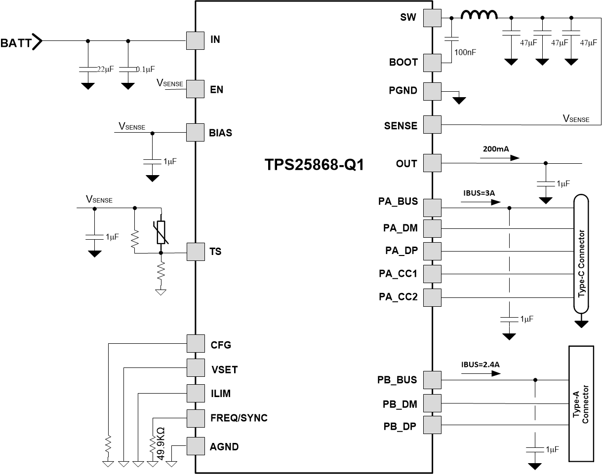
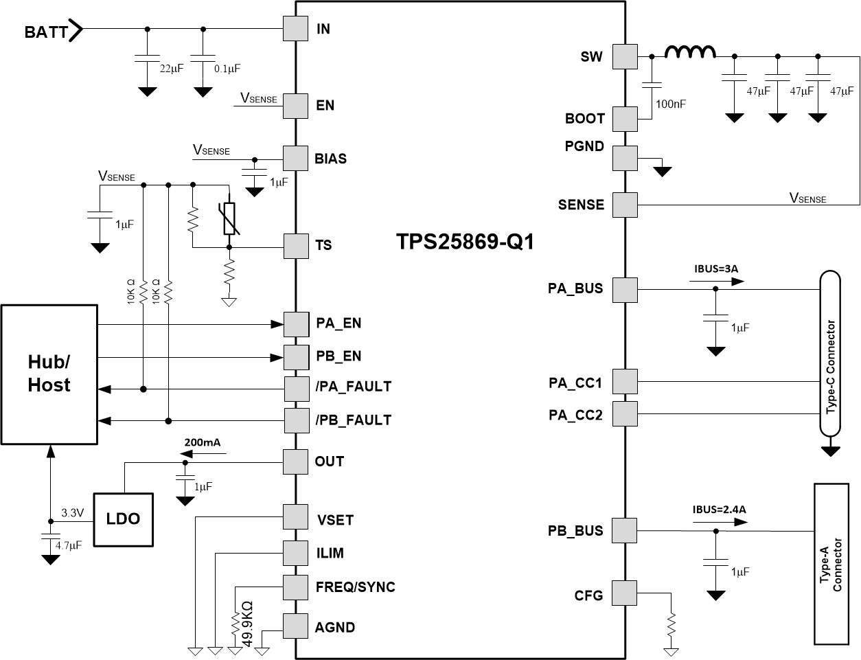
The TPS2586x-Q1 only requires a few external components to convert from a wide voltage range supply to a 5-V output to power USB devices. Figure 11-1 shows the TPS25868-Q1 typical application schematic for Dual Type-A and Type-C charging ports. Figure 11-2 shows the TPS25869-Q1 typical application schematic for Media HUB.
 Figure 11-1 TPS25868-Q1 Typical Application Circuit for
400-kHz fSW
 Figure 11-2 TPS25869-Q1 Typical Application Circuit for
400-kHz fSW
Figure 11-2 TPS25869-Q1 Typical Application Circuit for
400-kHz fSWAs a quick start guide, Table 11-1 provides typical component values for some of the most common configurations. The values given in Table 11-1 are typical. Other values can be used to enhance certain performance criterion as required by the application. The integrated buck regulator of TPS2586x-Q1 is internally compensated and optimized for a reasonable selection of external inductance and capacitance. The external components have to fulfill the needs of the application, but also the stability criteria of the control loop of the device.
| fSW | VOUT WITHOUT CABLE COMPENSATION | L | CHF + CIN | CBOOT | RATED COUT |
|---|---|---|---|---|---|
| 400 KHZ | 5.17 V | 3.3 µH | 1 X 100 nF + 1 × 47 µF | 1 × 100 nF | 3 × 47 µF |
- The inductance value is calculated based on max VIN = 18 V.
- All the COUT values are after derating and use low ESR ceramic capacitors.
- The COUT is the buck regulator output capacitors at the SENSE pin.