ZHCSCQ0 August   2014 TPS25921A , TPS25921L

PRODUCTION DATA.  

  1. 特性
  2. 应用范围
  3. 说明
  4. 应用电路原理图
  5. 修订历史记录
  6. Pin Configuration and Functions
  7. Specifications
    1. 7.1 Absolute Maximum Ratings
    2. 7.2 Handling Ratings
    3. 7.3 Recommended Operating Conditions
    4. 7.4 Thermal Characteristics
    5. 7.5 Electrical Characteristics
    6. 7.6 Timing Requirements
    7. 7.7 Typical Characteristics
  8. Parametric Measurement Information
  9. Detailed Description
    1. 9.1 Overview
    2. 9.2 Functional Block Diagram
    3. 9.3 Feature Description
      1. 9.3.1 Enable and Adjusting Undervoltage Lockout (UVLO)
      2. 9.3.2 Overvoltage Protection (OVP)
      3. 9.3.3 Hot Plug-in and In-Rush Current Control
      4. 9.3.4 Overload and Short Circuit Protection :
        1. 9.3.4.1 Overload Protection
        2. 9.3.4.2 Short Circuit Protection
        3. 9.3.4.3 Start-Up with Short on Output
        4. 9.3.4.4 Constant Current Limit Behavior during Overcurrent Faults
      5. 9.3.5 FAULT Response
      6. 9.3.6 IN, OUT and GND Pins
      7. 9.3.7 Thermal Shutdown:
    4. 9.4 Device Functional Modes
      1. 9.4.1 Shutdown Control
      2. 9.4.2 Operational Overview of Device Functions
  10. 10Applications and Implementation
    1. 10.1 Application Information
    2. 10.2 Typical Application
      1. 10.2.1 Precision Current Limiting and Protection for White Goods
        1. 10.2.1.1 Design Requirements
        2. 10.2.1.2 Detailed Design Procedure
          1. 10.2.1.2.1 Step by Step Design Procedure
          2. 10.2.1.2.2 Programming the Current-Limit Threshold: R(ILIM) Selection
          3. 10.2.1.2.3 Undervoltage Lockout and Overvoltage Set Point
          4. 10.2.1.2.4 Setting Output Voltage Ramp time (tSS)
            1. 10.2.1.2.4.1 Case1: Start-up Without Load: Only Output Capacitance C(OUT) Draws Current During Start-up
            2. 10.2.1.2.4.2 Case 2: Start-up With Load: Output Capacitance C(OUT) and Load Draws Current During Start-up
          5. 10.2.1.2.5 Support Component Selections - R4 and CIN
        3. 10.2.1.3 Application Curves
  11. 11System Examples
    1. 11.1 Protection and Current Limiting for Primary-Side Regulated Power Supplies
    2. 11.2 Precision Current Limiting in Intrinsic Safety Applications
    3. 11.3 Smart Load Switch
  12. 12Power Supply Recommendations
    1. 12.1 Transient Protection
    2. 12.2 Output Short-Circuit Measurements
  13. 13Layout
    1. 13.1 Layout Guidelines
    2. 13.2 Layout Example
  14. 14器件和文档支持
    1. 14.1 相关链接
    2. 14.2 Trademarks
    3. 14.3 Electrostatic Discharge Caution
    4. 14.4 术语表
  15. 15机械封装和可订购信息

封装选项

机械数据 (封装 | 引脚)
散热焊盘机械数据 (封装 | 引脚)
订购信息

6 Pin Configuration and Functions

SOIC (D) 8 PIN PACKAGE
(TOP VIEW)
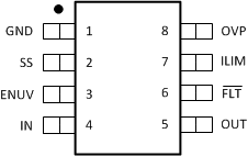
po_slvsce1.gif

Pin Functions

NAME NUMBER DESCRIPTION
GND 1 Ground.
SS 2 A capacitor from this pin to GND sets the ramp rate of output voltage at device turn-on.
ENUV 3 Input for setting programmable undervoltage lockout threshold. An undervoltage event will open internal FET and assert FLT to indicate power-failure. When pulled to GND, resets the thermal fault latch in TPS25921L.
IN 4 Power Input and supply voltage of the device.
OUT 5 Power Output of the device.
FLT 6 Fault event indicator, goes low to indicate fault condition due to Undervoltage, Overvoltage, and Thermal shutdown event. A nuisance fast trip does not trigger fault. It is an open drain output.
ILIM 7 A resistor from this pin to GND will set the overload and short circuit limit.
OVP 8 Input for setting programmable overvoltage protection threshold. An overvoltage event will open the internal FET and assert FLT to indicate overvoltage.