ZHCSE39A August 2015 – August 2015
PRODUCTION DATA.
- 1 特性
- 2 应用
- 3 说明
- 4 修订历史记录
- 5 Device Comparison Table
- 6 Pin Configuration and Functions
- 7 Specifications
- 8 Detailed Description
-
9 Application and Implementation
- 9.1 Application Information
- 9.2
Typical Applications
- 9.2.1
Simple 3.7-A eFuse Protection for Set Top Boxes
- 9.2.1.1 Design Requirements
- 9.2.1.2 Detailed Design Procedure
- 9.2.1.3 Application Curves
- 9.2.2 Inrush and Reverse Current Protection for Hold-Up Capacitor Application (for example, SSD)
- 9.2.1
Simple 3.7-A eFuse Protection for Set Top Boxes
- 10Power Supply Recommendations
- 11Layout
- 12器件和文档支持
- 13机械、封装和可订购信息
8 Detailed Description
8.1 Overview
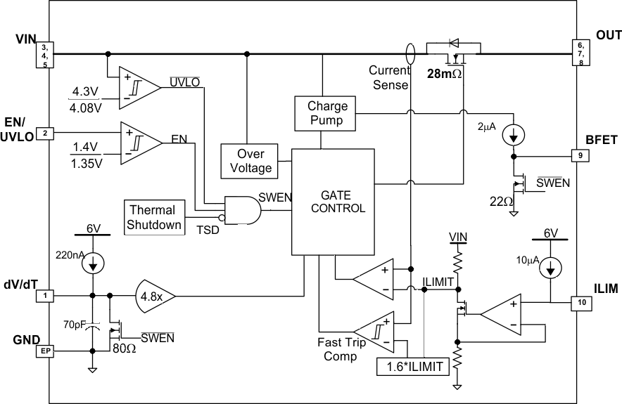
The TPS25923x is an e-fuse with integrated power switch that is used to manage current/voltage/start-up voltage ramp to a connected load. The device starts its operation by monitoring the VIN bus. When VIN exceeds the undervoltage-lockout threshold (VUVR), the device samples the EN/UVLO pin. A high level on this pin enables the internal MOSFET. As VIN rises, the internal MOSFET of the device will start conducting and allow current to flow from VIN to OUT. When EN/UVLO is held low (below VENF), internal MOSFET is turned off. User also has the ability to modify the output voltage ramp time by connecting a capacitor between dV/dT pin and GND.
After a successful start-up sequence, the device now actively monitors its load current and input voltage, ensuring that the adjustable overload current limit IOL is not exceeded and input voltage spikes are safely clamped to VOVC level at the output. This keeps the output device safe from harmful voltage and current transients. The device also has built-in thermal sensor. In the event device temperature (TJ) exceeds TSHDN, typically 150°C, the thermal shutdown circuitry will shut down the internal MOSFET thereby disconnecting the load from the supply. In TPS259230, the output will remain disconnected (MOSFET open) until power to device is recycled or EN/UVLO is toggled (pulled low and then high). The TPS259231 device will remain off during a cooling period until device temperature falls below TSHDN – 10°C, after which it will attempt to restart. This ON and OFF cycle will continue until fault is cleared.
8.2 Functional Block Diagram

8.3 Feature Description
8.3.1 GND
This is the most negative voltage in the circuit and is used as a reference for all voltage measurements unless otherwise specified.
8.3.2 VIN
Input voltage to the TPS25923x. A ceramic bypass capacitor close to the device from VIN to GND is recommended to alleviate bus transients. The recommended operating voltage range is 4.5 V to 5.5 V for TPS25923x. The device can continuously sustain a voltage of 20 V on VIN pin. However, above the recommended maximum bus voltage, the device will be in over-voltage protection (OVP) mode, limiting the output voltage to VOVC. The power dissipation in OVP mode is PD_OVP = (VVIN - VOVC) x IOUT, which can potentially heat up the device and cause thermal shutdown.
8.3.3 dV/dT
Connect a capacitor from this pin to GND to control the slew rate of the output voltage at power-on. This pin can be left floating to obtain a predetermined slew rate (minimum TdVdT) on the output. Equation governing slew rate at start-up is shown below:
Where:
IdVdT = 220 nA (TYP)
CINT = 70 pF (TYP)
GAINdVdT = 4.85
The total ramp time (TdVdT) for 0 to VIN can be calculated using the following equation:
For details on how to select an appropriate charging time/rate, refer to the applications section Setting Output Voltage Ramp Time (TdVdT).
8.3.4 BFET
Connect this pin to an external NFET that can be used to disconnect input supply from rest of the system in the event of power failure at VIN. The BFET pin is controlled by either input UVLO (VUVR) event or EN/UVLO (see Table 1). BFET can source charging current of 2 µA (TYP) and sink (discharge) current from the gate of the external FET via a 26-Ω internal discharge resistor to initiate fast turn-off, typically <1 µs. Due to 2 µA charging current, it is recommended to use >10 MΩ impedance when probing the BFET node.
Table 1. BFET
| EN/UVLO > VENR | VIN > VUVR | BFET MODE |
|---|---|---|
| H | H | Charge |
| X | L | Discharge |
| L | X | Discharge |
8.3.5 EN/UVLO
As an input pin, it controls both the ON/OFF state of the internal MOSFET and that of the external blocking FET. In its high state, the internal MOSFET is enabled and charging begins for the gate of external FET. A low on this pin will turn off the internal MOSFET and pull the gate of the external FET to GND via the built-in discharge resistor. High and Low levels are specified in the parametric table of the datasheet. The EN/UVLO pin is also used to clear a thermal shutdown latch in the TPS259230 by toggling this pin (H→L).
The internal de-glitch delay on EN/UVLO falling edge is intentionally kept low (1 us typical) for quick detection of power failure. When used with a resistor divider from supply to EN/UVLO to GND, power-fail detection on EN/UVLO helps in quick turn-off of the BFET driver, thereby stopping the flow of reverse current (see typical application diagram, Figure 43). For applications where a higher de-glitch delay on EN/UVLO is desired, or when the supply is particularly noisy, it is recommended to use an external bypass capacitor from EN/UVLO to GND.
8.3.6 ILIM
The device continuously monitors the load current and keeps it limited to the value programmed by RILIM. After start-up event and during normal operation, current limit is set to IOL (over-load current limit).

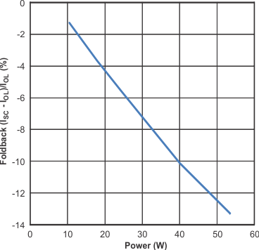
When power dissipation in the internal MOSFET [PD = (VVIN – VOUT) × IOUT] exceeds 10 W, there is a 2% – 12% thermal foldback in the current limit value so that IOL drops to ISC. In each of the two modes, MOSFET gate voltage is regulated to throttle short-circuit and overload current flowing to the load. Eventually, the device shuts down due to over temperature.
 Figure 36. Thermal Foldback in Current Limit
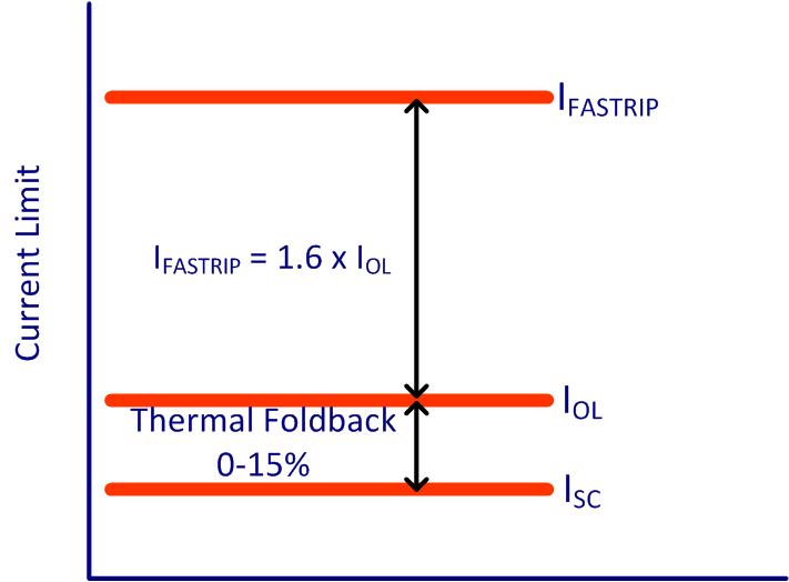
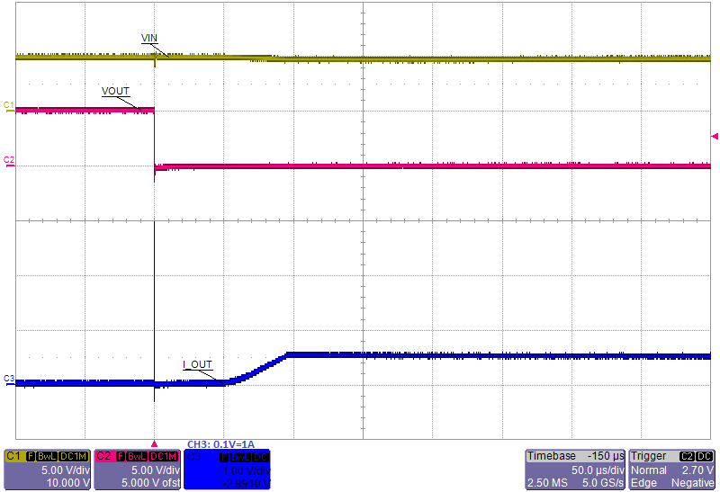
During a transient short circuit event, the current through the device increases very rapidly. The current-limit amplifier cannot respond very quickly to this event due to its limited bandwidth. Therefore, the TPS2592 incorporates a fast-trip comparator, which shuts down the pass device very quickly when IOUT > IFASTRIP, and terminates the rapid short-circuit peak current. The trip threshold is set to 60% higher than the programmed over-load current limit (IFASTRIP = 1.6 x IOL). After the transient short-circuit peak current has been terminated by the fast-trip comparator, the current limit amplifier smoothly regulates the output current to IOL (see figure below).
 Figure 37. Fast-Trip Current
 Figure 38. Fast-Trip and Current Limit Amplifier Response for Short Circuit
8.4 Device Functional Modes
The TPS25923x is a hot-swap controller with integrated power switch that is used to manage current/voltage/start-up voltage ramp to a connected load. The device starts its operation by monitoring the VIN bus. When VVIN exceeds the undervoltage-lockout threshold (VUVR), the device samples the EN/UVLO pin. A high level on this pin enables the internal MOSFET and also start charging the gate of external blocking FET (if connected) via the BFET pin. As VIN rises, the internal MOSFET of the device and external FET (if connected) will start conducting and allow current to flow from VIN to OUT. When EN/UVLO is held low (that is, below VENF), the internal MOSFET is turned off and BFET pin is discharged, thereby, blocking the flow of current from VIN to OUT. User also has the ability to modify the output voltage ramp time by connecting a capacitor between dV/dT pin and GND.
Having successfully completed its start-up sequence, the device now actively monitors its load current and input voltage, ensuring that the adjustable overload current limit IOL is not exceeded and input voltage spikes are safely clamped to VOVC level at the output. This keeps the output device safe from harmful voltage and current transients. The device also has built-in thermal sensor. In the event device temperature (TJ) exceeds TSHDN , typically 150°C, the thermal shutdown circuitry will shut down the internal MOSFET thereby disconnecting the load from the supply. In the TPS259230, the output will remain disconnected (MOSFET open) until power to device is recycled or EN/UVLO is toggled (pulled low and then high). The TPS259231 device will remain off during a cooling period until device temperature falls below TSHDN – 10°C, after which it will attempt to restart. This ON and OFF cycle will continue until fault is cleared.

