ZHCSE34A August   2015  – August 2015

PRODUCTION DATA.  

  1. 特性
  2. 应用
  3. 说明
  4. 修订历史记录
  5. Device Comparison Table
  6. Pin Configuration and Functions
  7. Specifications
    1. 7.1 Absolute Maximum Ratings
    2. 7.2 ESD Ratings
    3. 7.3 Recommended Operating Conditions
    4. 7.4 Thermal Information
    5. 7.5 Electrical Characteristics
    6. 7.6 Timing Requirements
    7. 7.7 Typical Characteristics
  8. Detailed Description
    1. 8.1 Overview
    2. 8.2 Functional Block Diagram
    3. 8.3 Feature Description
      1. 8.3.1 GND
      2. 8.3.2 VIN
      3. 8.3.3 dV/dT
      4. 8.3.4 EN/UVLO
      5. 8.3.5 ILIM
    4. 8.4 Device Functional Modes
  9. Application and Implementation
    1. 9.1 Application Information
    2. 9.2 Typical Application
      1. 9.2.1 Simple eFuse Protection for Set Top Boxes
        1. 9.2.1.1 Design Requirements
        2. 9.2.1.2 Detailed Design Procedure
          1. 9.2.1.2.1 Step by Step Design Procedure
          2. 9.2.1.2.2 Programming the Current-Limit Threshold: RILIM Selection
          3. 9.2.1.2.3 Undervoltage Lockout Set Point
          4. 9.2.1.2.4 Setting Output Voltage Ramp Time (TdVdT)
            1. 9.2.1.2.4.1 Case 1: Start-Up without Load: Only Output Capacitance COUT Draws Current During Start-Up
            2. 9.2.1.2.4.2 Case 2: Start-Up with Load: Output Capacitance COUT and Load Draws Current During Start-Up
          5. 9.2.1.2.5 Support Component Selection - CVIN
        3. 9.2.1.3 Application Curves
  10. 10Power Supply Recommendations
    1. 10.1 Transient Protection
    2. 10.2 Output Short-Circuit Measurements
  11. 11Layout
    1. 11.1 Layout Guidelines
    2. 11.2 Layout Example
  12. 12器件和文档支持
    1. 12.1 器件支持
      1. 12.1.1 Third-Party Products Disclaimer
    2. 12.2 文档支持
      1. 12.2.1 相关文档
    3. 12.3 相关链接
    4. 12.4 社区资源
    5. 12.5 商标
    6. 12.6 静电放电警告
    7. 12.7 Glossary
  13. 13机械、封装和可订购信息

封装选项

机械数据 (封装 | 引脚)
散热焊盘机械数据 (封装 | 引脚)
订购信息

6 Pin Configuration and Functions

DRC Package
10-Pin VSON
Top View
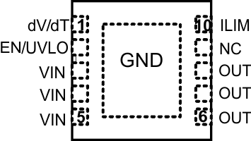
TPS259250 TPS259251 TPS259260 TPS259261 pin_out_top_SLVSCQ3.gif

Pin Functions

PIN DESCRIPTION
NAME NUMBER
dV/dT 1 Connect a capacitor from this pin to GND to control the ramp rate of OUT voltage at device turn-on.
EN/UVLO 2 This is a dual function control pin. When used as an ENABLE pin and pulled down, it shuts off the internal pass MOSFET. When pulled high, it enables the device.
As an UVLO pin, it can be used to program different UVLO trip point via external resistor divider.
GND Thermal Pad GND
ILIM 10 A resistor from this pin to GND will set the overload and short circuit limit.
NC 9 Not Connected Internally. Can be left floating or grounded.
OUT 6-8 Output of the device
VIN 3-5 Input supply voltage