ZHCSF29E May 2016 – January 2021 TPS25940-Q1
PRODMIX
- 1 特性
- 2 应用
- 3 说明
- 4 Revision History
- 5 Device Comparison Table
- 6 Pin Configuration and Functions
- 7 Specifications
- 8 Parametric Measurement Information
-
9 Detailed Description
- 9.1 Overview
- 9.2 Functional Block Diagram
- 9.3 Feature Description
- 9.4 Device Functional Modes
-
10Application and Implementation
- 10.1 Application Information
- 10.2
Typical Application
- 10.2.1 Design Requirements
- 10.2.2
Detailed Design Procedure
- 10.2.2.1 Step by Step Design Procedure
- 10.2.2.2 Programming the Current-Limit Threshold: R(ILIM) Selection
- 10.2.2.3 Undervoltage Lockout and Overvoltage Set Point
- 10.2.2.4 Programming Current Monitoring Resistor—RIMON
- 10.2.2.5 Setting Output Voltage Ramp Time (tdVdT)
- 10.2.2.6 Programing the Power Good Set Point
- 10.2.2.7 Support Component Selections—R6, R7 and CIN
- 10.2.3 Application Curves
- 10.2.4 System Examples
- 11Power Supply Recommendations
- 12Layout
- 13Device and Documentation Support
- 14Mechanical, Packaging, and Orderable Information
10.2.4.2 Power Failure Protection for Holdup Power
For certain applications, it is necessary to have hold-up circuit and capacitor bank to ensure that critical user data is never lost during power-failure to the drive. The power-failure event could be because of the momentary loss of power regulation (transient brown-out condition) or because of the loss of power when system is hot-plugged out.
The TPS25940xx-Q1 device continuously monitors the supply voltage at EN/UVLO pin and swiftly disconnects the input bus from output when the voltage drops below a predefined threshold (power fail detection). Reverse current flow from output side to input supply gets blocked when reverse voltage from IN to OUT exceeds –66 mV. In addition, it provides an instant warning signal ( FLT) to the controller. Its swift true reverse blocking feature reacts in 1 µs (typical) ensuring that the capacitor bank charge is retained. This helps the drive to have power for longer time to harden data and reduces the capacitance required in the hold-up bank, saving system cost.
The typical application diagram of TPS25940xx-Q1 usage for holdup power is shown in Figure 10-23.

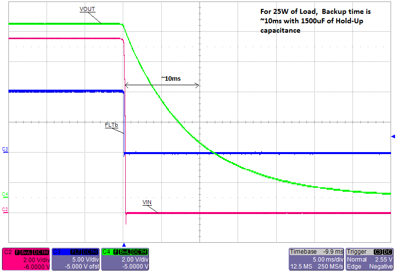
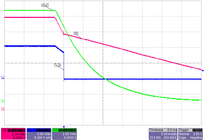
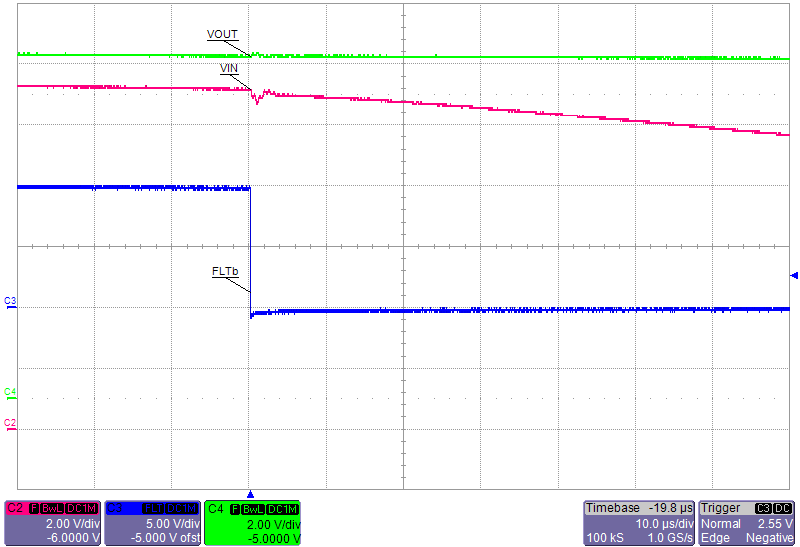
The oscilloscope plots demonstrating the true reverse blocking, fast turn-off and FLT signal delay are shown in Figure 10-24 through Figure 10-26.

| V(IN) = 12 V | C(OUT) = 1500 µF | RL = 5.6 Ω |

| V(IN) = 12 V | C(OUT) = 1500 µF | RL = 5.6 Ω |

| V(IN) = 12 V | C(OUT) = 1500 µF | RL = 5.6 Ω |