ZHCSCK2 June   2014

PRODUCTION DATA.  

  1. 特性
  2. 应用范围
  3. 说明
  4. 简化电路原理图
  5. 修订历史记录
  6. Pin Configuration and Functions
  7. Specifications
    1. 7.1 Absolute Maximum Ratings
    2. 7.2 Handling Ratings
    3. 7.3 Recommended Operating Conditions
    4. 7.4 Thermal Characteristics
    5. 7.5 Electrical Characteristics
    6. 7.6 Timing Requirements
    7. 7.7 Typical Characteristics
  8. Parametric Measurement Information
  9. Detailed Description
    1. 9.1 Overview
    2. 9.2 Functional Block Diagram
    3. 9.3 Feature Description
      1. 9.3.1 Enable and Adjusting Undervoltage Lockout
      2. 9.3.2 Overvoltage Protection (OVP)
      3. 9.3.3 Hot Plug-in and In-Rush Current Control
      4. 9.3.4 Overload and Short Circuit Protection :
        1. 9.3.4.1 Overload Protection
        2. 9.3.4.2 Short Circuit Protection
        3. 9.3.4.3 Start-Up with Short on Output
        4. 9.3.4.4 Constant Current Limit Behavior During Overcurrent Faults
      5. 9.3.5 FAULT Response
      6. 9.3.6 Current Monitoring:
      7. 9.3.7 Power Good Comparator
      8. 9.3.8 IN, OUT and GND Pins
      9. 9.3.9 Thermal Shutdown:
    4. 9.4 Device Functional Modes
      1. 9.4.1 DevSleep Mode for SATA® Interface Devices
      2. 9.4.2 Shutdown Control
  10. 10Application and Implementation
    1. 10.1 Application Information
    2. 10.2 Typical Application
      1. 10.2.1 eFuse for Enterprise SSDs
        1. 10.2.1.1 Design Requirements
        2. 10.2.1.2 Detailed Design Procedure
          1. 10.2.1.2.1 Step by Step Design Procedure
          2. 10.2.1.2.2 Programming the Current-Limit Threshold: R(ILIM) Selection
          3. 10.2.1.2.3 Undervoltage Lockout and Overvoltage Set Point
          4. 10.2.1.2.4 Programming Current Monitoring Resistor - RIMON
          5. 10.2.1.2.5 Setting Output Voltage Ramp time (tdVdT)
            1. 10.2.1.2.5.1 Case1: Start-up Without Load: Only Output Capacitance C(OUT) Draws Current During Start-up
            2. 10.2.1.2.5.2 Case 2: Start-up With Load: Output Capacitance C(OUT) and Load Draws Current During Start-up
          6. 10.2.1.2.6 Programing the Power Good Set Point
          7. 10.2.1.2.7 Support Component Selections - R6, R7 and CIN
        3. 10.2.1.3 Application Curves
    3. 10.3 System Examples
      1. 10.3.1 Power Failure Protection and Data Retention in SSDs
      2. 10.3.2 Boost Power Rail Configuration for Data Retention in Enterprise SSDs
  11. 11Power Supply Recommendations
    1. 11.1 Transient Protection
    2. 11.2 Output Short-Circuit Measurements
  12. 12Layout
    1. 12.1 Layout Guidelines
    2. 12.2 Layout Example
  13. 13器件和文档支持
    1. 13.1 相关链接
    2. 13.2 Trademarks
    3. 13.3 Electrostatic Discharge Caution
    4. 13.4 Glossary
  14. 14机械封装和可订购信息

封装选项

请参考 PDF 数据表获取器件具体的封装图。

机械数据 (封装 | 引脚)
  • RVC|20
散热焊盘机械数据 (封装 | 引脚)
订购信息

8 Parametric Measurement Information
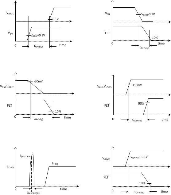
Parametric_Diagrams_slvsce9.gifFigure 42. Timing Diagrams