ZHCSCJ3D June 2014 – October 2017 TPS25942A , TPS25942L , TPS25944A , TPS25944L
UNLESS OTHERWISE NOTED, this document contains PRODUCTION DATA.
- 1 特性
- 2 应用范围
- 3 说明
- 4 修订历史记录
- 5 Device Comparison Table
- 6 Pin Configuration and Functions
- 7 Specifications
- 8 Parameter Measurement Information
-
9 Detailed Description
- 9.1 Overview
- 9.2 Functional Block Diagram
- 9.3
Feature Description
- 9.3.1 Enable and Adjusting Undervoltage Lockout
- 9.3.2 Overvoltage Protection (OVP)
- 9.3.3 Hot Plug-In and In-Rush Current Control
- 9.3.4 Overload and Short Circuit Protection
- 9.3.5 Reverse Current Protection
- 9.3.6 FAULT Response
- 9.3.7 Current Monitoring
- 9.3.8 Power Good Comparator
- 9.3.9 IN, OUT and GND Pins
- 9.3.10 Thermal Shutdown
- 9.4 Device Functional Modes
-
10Application and Implementation
- 10.1 Application Information
- 10.2
Typical Application
- 10.2.1 Design Requirements
- 10.2.2
Detailed Design Procedure
- 10.2.2.1 Step by Step Design Procedure
- 10.2.2.2 Programming the Current-Limit Threshold: R(ILIM) Selection
- 10.2.2.3 Undervoltage Lockout and Overvoltage Set Point
- 10.2.2.4 Programming Current Monitoring Resistor—RIMON
- 10.2.2.5 Setting Output Voltage Ramp Time (tdVdT)
- 10.2.2.6 Programing the Power Good Set Point
- 10.2.2.7 Support Component Selections—R6, R7 and CIN
- 10.2.3 Application Curves
- 10.3 System Examples
- 11Power Supply Recommendations
- 12Layout
- 13器件和文档支持
- 14机械、封装和可订购信息
11 Power Supply Recommendations
The devices are designed for supply voltage range of 2.7 V ≤ VIN ≤ 18 V. If the input supply is located more than a few inches from the device an input ceramic bypass capacitor higher than 0.1 μF is recommended. Power supply must be rated higher than the current limit set to avoid voltage droops during over current and short-circuit conditions.
11.1 Transient Protection
In case of short circuit and over load current limit, when the device interrupts current flow, input inductance generates a positive voltage spike on the input and output inductance generates a negative voltage spike on the output. The peak amplitude of voltage spikes (transients) is dependent on value of inductance in series to the input or output of the device. Such transients can exceed the Absolute Maximum Ratings of the device if steps are not taken to address the issue.
Typical methods for addressing transients include
- Minimizing lead length and inductance into and out of the device
- Using large PCB GND plane
- Schottky diode across the output to absorb negative spikes
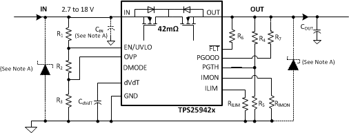
- A low value ceramic capacitor (C(IN) = 0.001 µF to 0.1 µF) to absorb the energy and dampen the transients. The approximate value of input capacitance can be estimated with Equation 37.

where
- V(IN) is the nominal supply voltage
- I(LOAD) is the load current,
- L(IN) equals the effective inductance seen looking into the source
- C(IN) is the capacitance present at the input
Some applications may require the addition of a Transient Voltage Suppressor (TVS) to prevent transients from exceeding the Absolute Maximum Ratings of the device.
The circuit implementation with optional protection components (a ceramic capacitor, TVS and schottky diode) is shown in Figure 87.

11.2 Output Short-Circuit Measurements
It is difficult to obtain repeatable and similar short-circuit testing results. Source bypassing, input leads, circuit layout and component selection, output shorting method, relative location of the short, and instrumentation all contribute to variation in results. The actual short itself exhibits a certain degree of randomness as it microscopically bounces and arcs. Care in configuration and methods must be used to obtain realistic results. Do not expect to see waveforms exactly like those in the data sheet; every setup differs.