ZHCSCJ3D June 2014 – October 2017 TPS25942A , TPS25942L , TPS25944A , TPS25944L
UNLESS OTHERWISE NOTED, this document contains PRODUCTION DATA.
- 1 特性
- 2 应用范围
- 3 说明
- 4 修订历史记录
- 5 Device Comparison Table
- 6 Pin Configuration and Functions
- 7 Specifications
- 8 Parameter Measurement Information
-
9 Detailed Description
- 9.1 Overview
- 9.2 Functional Block Diagram
- 9.3
Feature Description
- 9.3.1 Enable and Adjusting Undervoltage Lockout
- 9.3.2 Overvoltage Protection (OVP)
- 9.3.3 Hot Plug-In and In-Rush Current Control
- 9.3.4 Overload and Short Circuit Protection
- 9.3.5 Reverse Current Protection
- 9.3.6 FAULT Response
- 9.3.7 Current Monitoring
- 9.3.8 Power Good Comparator
- 9.3.9 IN, OUT and GND Pins
- 9.3.10 Thermal Shutdown
- 9.4 Device Functional Modes
-
10Application and Implementation
- 10.1 Application Information
- 10.2
Typical Application
- 10.2.1 Design Requirements
- 10.2.2
Detailed Design Procedure
- 10.2.2.1 Step by Step Design Procedure
- 10.2.2.2 Programming the Current-Limit Threshold: R(ILIM) Selection
- 10.2.2.3 Undervoltage Lockout and Overvoltage Set Point
- 10.2.2.4 Programming Current Monitoring Resistor—RIMON
- 10.2.2.5 Setting Output Voltage Ramp Time (tdVdT)
- 10.2.2.6 Programing the Power Good Set Point
- 10.2.2.7 Support Component Selections—R6, R7 and CIN
- 10.2.3 Application Curves
- 10.3 System Examples
- 11Power Supply Recommendations
- 12Layout
- 13器件和文档支持
- 14机械、封装和可订购信息
10 Application and Implementation
NOTE
Information in the following applications sections is not part of the TI component specification, and TI does not warrant its accuracy or completeness. TI’s customers are responsible for determining suitability of components for their purposes. Customers should validate and test their design implementation to confirm system functionality.
10.1 Application Information
The device is a smart eFuse. It is typically used for Active ORing and Power Multiplexing applications. It operates from 2.7 V to 18 V with programmable current limit, overvoltage and undervoltage protection. The device aids in controlling the in-rush current and in seamless power path management of multiple voltage rails for systems such as PCIe cards, Network and Graphic Cards and SSDs. The device also provides robust protection for multiple faults on the sub-system rail.
The following design procedure can be used to select component values for the TPS25942, TPS25944.
Alternatively, the WEBENCH® software may be used to generate a complete design. The WEBENCH® software uses an iterative design procedure and accesses a comprehensive database of components when generating a design. Additionally, a spreadsheet design tool TPS25942_44 Design Calculator is available on web folder.
This section presents a simplified discussion of the design process.
10.2 Typical Application
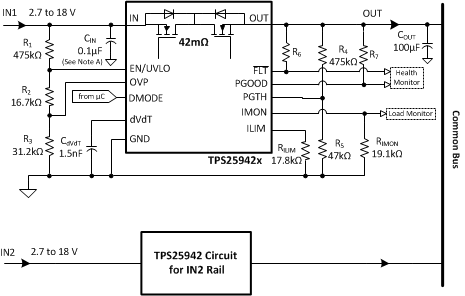
10.2.1 Design Requirements
Table 2 lists the TPS25942, TPS25944 design parameters.
Table 2. Design Parameters
| DESIGN PARAMETER | EXAMPLE VALUE |
|---|---|
| Input voltage, V(IN) | 12 V |
| Undervoltage lockout set point, V(UV) | 10.8 V |
| Overvoltage protection set point , V(OV) | 16.5 V |
| Load at start-up , RL(SU) | 4.8 Ω |
| Current limit, I(LIM) | 5 A |
| Load capacitance , C(OUT) | 100 µF |
| Maximum ambient temperatures , TA | 85°C |
10.2.2 Detailed Design Procedure
The following design procedure can be used to select component values for the TPS25942, TPS25944.
10.2.2.1 Step by Step Design Procedure
To begin the design process a few parameters must be decided upon. The designer needs to know the following:
- Normal input operation voltage
- Maximum output capacitance
- Maximum current Limit
- Load during start-up
- Maximum ambient temperature of operation
This design procedure below seeks to control the junction temperature of device under both static and transient conditions by proper selection of output ramp-up time and associated support components. The designer can adjust this procedure to fit the application and design criteria.
10.2.2.2 Programming the Current-Limit Threshold: R(ILIM) Selection
R(ILIM) sets the current limit. Using Equation 4.

Choose the closest standard value: 17.8k, 1% standard value resistor.
10.2.2.3 Undervoltage Lockout and Overvoltage Set Point
The undervoltage lockout (UVLO) and overvoltage trip point are adjusted using the external voltage divider network of R1, R2 and R3 as connected between IN, EN, OVP and GND pins of the TPS25942, TPS25944 devices. The values required for setting the undervoltage and overvoltage are calculated solving Equation 11 and Equation 12.

where
- V(OVPR) = OVP Threshold for rising voltage

where
- V(ENR) = Enable threshold for rising voltage
For minimizing the input current drawn from the power supply {I(R123) = V(IN)/(R1 + R2 + R3)}, it is recommended to use higher values of resistance for R1, R2 and R3.
However, leakage currents due to external active components connected to the resistor string can add error to these calculations. So, the resistor string current, I(R123) must be chosen to be 20x greater than the leakage current expected.
From the device electrical specifications, V(OVPR) = 0.99 V and V(ENR) = 0.99 V. For design requirements, V(OV) is 16.5 V and V(UV) is 10.8 V. To solve the equation, first choose the value of R3 = 31.2 kΩ and use Equation 11 to solve for (R1 + R2) = 488.8 kΩ. Use Equation 12 and value of (R1 + R2) to solve for R2 = 16.47 kΩ and finally R1= 472.33 kΩ.
Using the closest standard 1% resistor values gives R1 = 475 kΩ, R2 = 16.7 kΩ, and R3 = 31.2 kΩ.
The power fail threshold V(PFAIL) is detected on the falling edge of the power supply. The falling voltage threshold is 7% lower than the rising voltage threshold, so for a set V(UV) the power fail voltage V(PFAIL) is given by Equation 13.
10.2.2.4 Programming Current Monitoring Resistor—RIMON
Voltage at IMON pin V(IMON) represents the voltage proportional to load current. This can be connected to an ADC of the downstream system for health monitoring of the system. The R(IMON) need to be configured based on the maximum input voltage range of the ADC used. R(IMON) is set using Equation 14.

For I(LIM) = 5 A, and considering the operating range of ADC from 0 V to 5 V, V(IMONmax) is 5 V and R(IMON) is determined by Equation 15:

Selecting R(IMON) value less than determined by Equation 15 ensures that ADC limits are not exceeded for maximum value of load current.
If the IMON pin voltage is not being digitized with an ADC, R(IMON) can be selected to produce a 1V/1A voltage at the IMON pin, using Equation 14.
Choose closest 1 % standard value: 19.1 kΩ.
If current monitoring up to I(FASTRIP) is desired, R(IMON) can be reduced by a factor of 1.6, as in Equation 6.
10.2.2.5 Setting Output Voltage Ramp Time (tdVdT)
For a successful design, the junction temperature of device must be kept below the absolute-maximum rating during both dynamic (start-up) and steady state conditions. Dynamic power stresses often are an order of magnitude greater than the static stresses, so it is important to determine the right start-up time and in-rush current limit required with system capacitance to avoid thermal shutdown during start-up with and without load.
The ramp-up capacitor C(dVdT) needed is calculated considering the two possible cases:
10.2.2.5.1 Case1: Start-Up Without Load: Only Output Capacitance C(OUT) Draws Current During Start-Up
During start-up, as the output capacitor charges, the voltage difference across the internal FET decreases, and the power dissipated decreases as well. Typical ramp-up of output voltage V(OUT) with inrush current limit of 1.2 A and power dissipated in the device during start-up is shown in Figure 56. The average power dissipated in the device during start-up is equal to area of triangular plot (red curve in Figure 57) averaged over tdVdT.
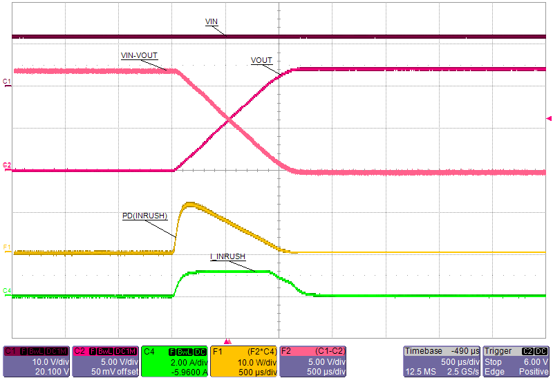
| V(IN) = 12 V | C(dVdT) = 1 nF | C(OUT) = 100 µF |
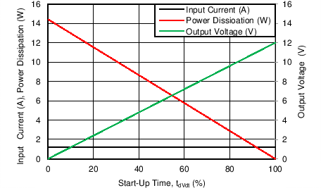
| V(IN) = 12 V | C(dVdT) = 1 nF | C(OUT) = 100 µF |
For the TPS25944, TPS25944 device, the inrush current is determined as shown in Equation 16.

Power dissipation during start-up is given by Equation 17.

Equation 17 assumes that load does not draw any current until the output voltage has reached its final value.
10.2.2.5.2 Case 2: Start-Up With Load: Output Capacitance C(OUT) and Load Draws Current During Start-Up
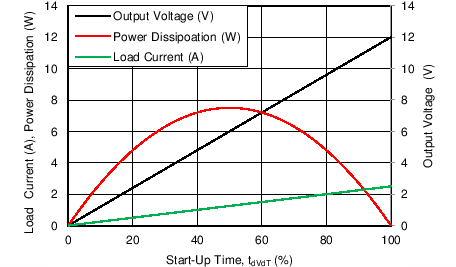
When load draws current during the turn-on sequence, there is additional power dissipated. Considering a resistive load RL(SU) during start-up, load current ramps up proportionally with increase in output voltage during tdVdT time. Typical ramp-up of output voltage, load current and power dissipated in the device is shown in Figure 58 and power dissipation with respect to time is plotted in Figure 59. The additional power dissipation during start-up phase is calculated as follows shown in Equation 18 and Equation 19.


Where RL(SU) is the load resistance present during start-up. Average energy loss in internal FET during charging time due to resistive load is given by Equation 20.

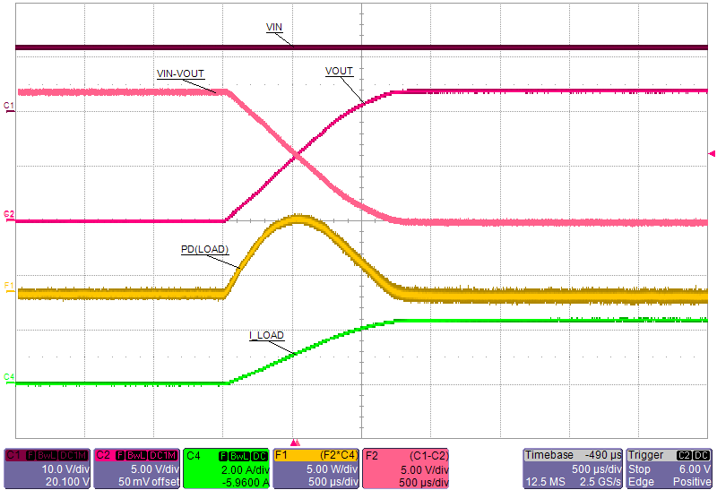
| V(IN) = 12 V | C(dVdT) = 1 nF, C(OUT) = 100 µF | RL(SU) = 4.8 Ω |
| V(IN) = 12 V | C(dVdT) = 1 nF, C(OUT) = 100 µF | RL(SU) = 4.8 Ω |
Solving Equation 20 the average power loss in the device due to load is given by Equation 21.

Total power dissipated in the device during start-up is given by Equation 22.

Total current during start-up is given by Equation 23.

If I(STARTUP) > I(LIM), the device limits the current to I(LIM) and the current limited charging time is determined by Equation 24.

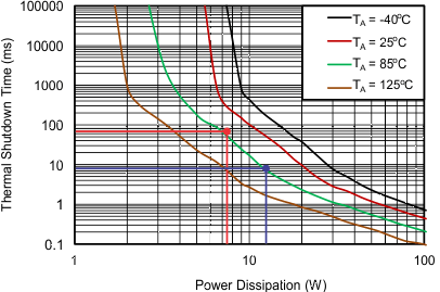
The power dissipation, with and without load, for selected start-up time must not exceed the shutdown limits as shown in Figure 60.
For the design example under discussion,
Select ramp-up capacitor C(dVdT) = 1nF, using Equation 2, we get Equation 25.

The inrush current drawn by the load capacitance (C(OUT)) during ramp-up is calculated using Equation 3 and Equation 26.

The inrush Power dissipation is calculated, using Equation 17 and Equation 27.

For 7.2 W of power loss, the thermal shut down time of the device must not be less than the ramp-up time tdVdT to avoid the false trip at maximum operating temperature. From thermal shutdown limit graph Figure 60 at TA = 85°C, for 7.2 W of power the shutdown time is approximately 60 ms. So it is safe to use 1 ms as start-up time without any load on output.
Considering the start-up with load 4.8 Ω, the additional power dissipation, when load is present during start-up is calculated, using Equation 21 and Equation 28.

The total device power dissipation during start up is given by Equation 29.

From thermal shutdown limit graph at TA = 85°C, the thermal shutdown time for 12.2 W is close to 7.5 ms. It is safe to have 30% margin to allow for variation of system parameters such as load, component tolerance, and input voltage. So it is well within acceptable limits to use the 1 nF capacitor with start-up load of 4.8 Ω.
If there is a need to decrease the power loss during start-up, it can be done with increase of C(dVdT) capacitor.
To illustrate, choose C(dVdT) = 1.5 nF as an option and recalculate as shown in Equation 30 to Equation 34.


From thermal shutdown limit graph at TA = 85°C, the shutdown time for 10 W power dissipation is approximately 17 ms, which increases the margins further for shutdown time and ensures successful operation during start-up and steady state conditions.
The spreadsheet tool available on the web can be used for iterative calculations.
10.2.2.6 Programing the Power Good Set Point
As shown in Figure 55, R4 and R5 sets the required limit for PGOOD signal as needed for the downstream converters. Considering a power good threshold of 11 V for this design, the values of R4 and R5 are calculated using Equation 35.

It is recommended to have high values for these resistors to limit the current drawn from the output node. Choosing a value of R4 = 475 kΩ, R5 = 47 kΩ provides V(PGTH) = 11 V.
10.2.2.7 Support Component Selections—R6, R7 and CIN
Reference to application schematics, R6 and R7 are required only if PGOOD and FLT are used; these resistors serve as pull-ups for the open-drain output drivers. The current sunk by each of these pins must not exceed 10 mA (see the Absolute Maximum Ratings table). CIN is a bypass capacitor to help control transient voltages, unit emissions, and local supply noise. Where acceptable, a value in the range of 0.001 μF to 0.1 μF is recommended for CIN.
10.2.3 Application Curves
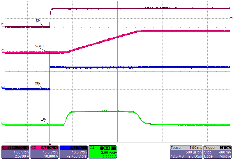 Figure 61. Hot-Plug Start-Up: Output Ramp Without Load on Output
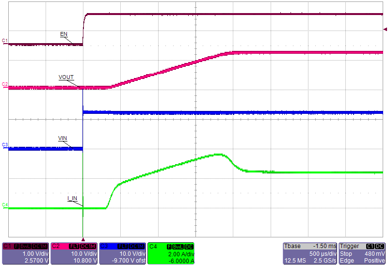 Figure 62. Hot-Plug Start-Up: Output Ramp With Start-Up load of 4.8 Ω
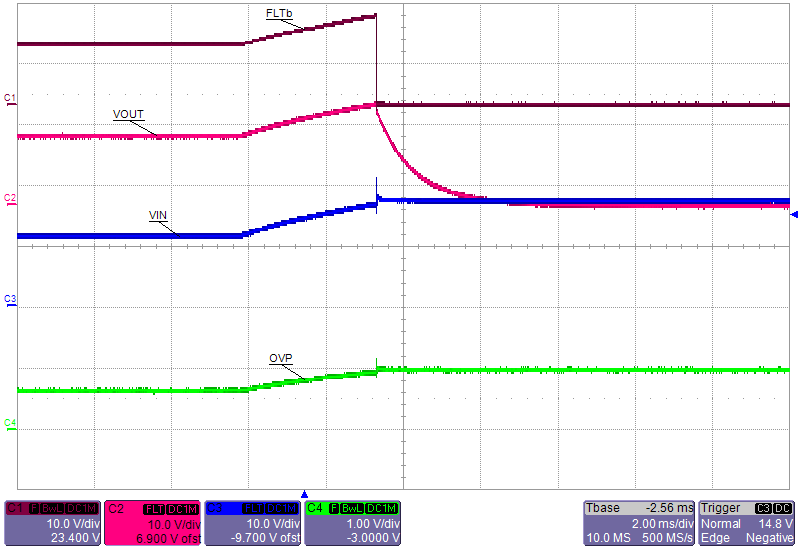 Figure 63. Overvoltage Shutdown
 Figure 65. Over Load: Step Change in Load From 12 Ω to 2 Ω and Back
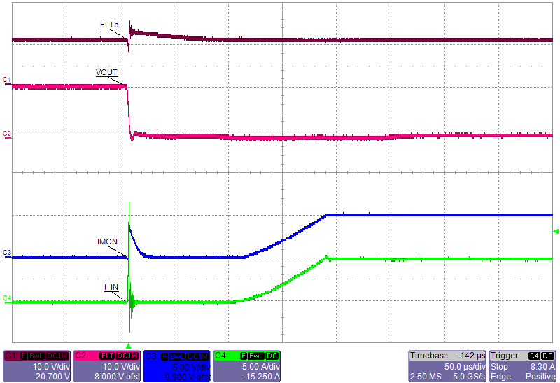 Figure 67. Hot Short: Fast Trip and Current Regulation
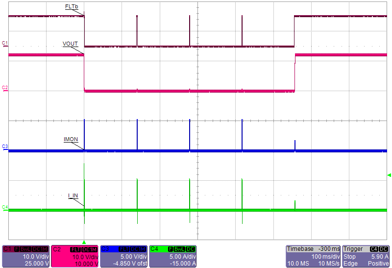 Figure 69. Hot Short: Auto-Retry and Recovery from Short Circuit—TPS25942A
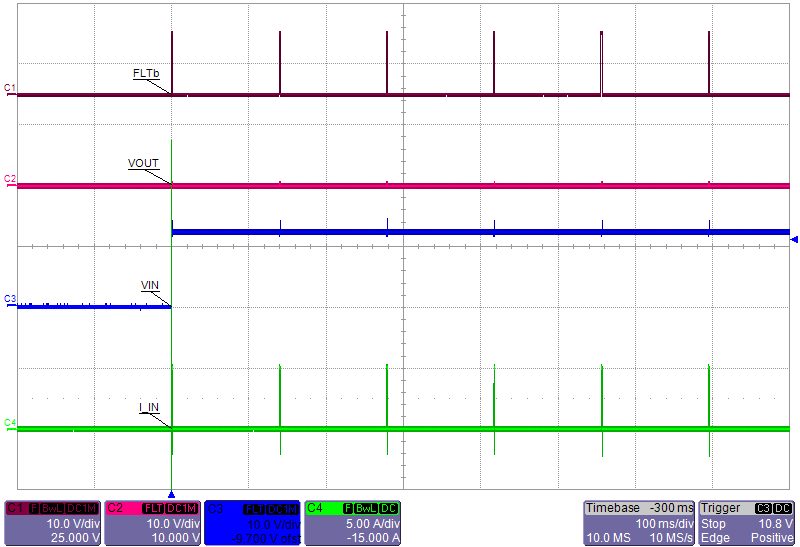 Figure 71. Hot Plug-In With Short on Output: Auto-Retry—TPS25942A
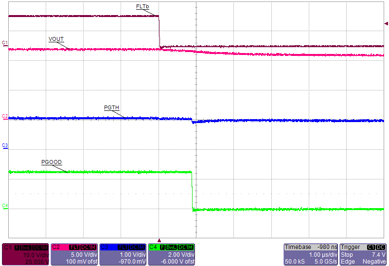 Figure 73. Power Good Response During Turnoff
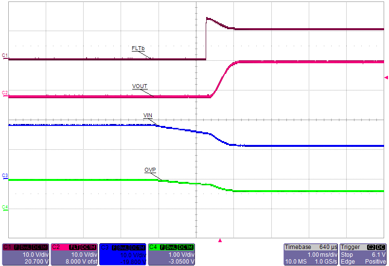 Figure 64. Overvoltage Recovery
 Figure 66. Overload Condition: Auto Retry and Recovery—TPS25942A
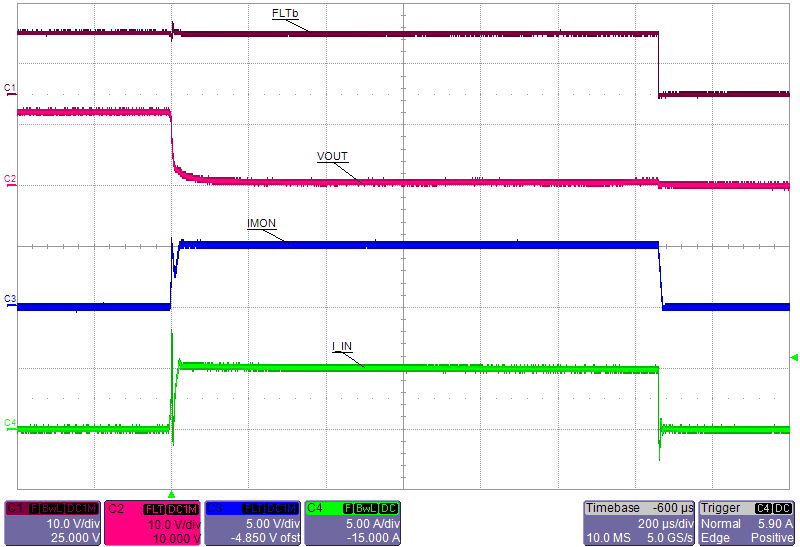 Figure 68. Hot Short: Latched—TPS25942L
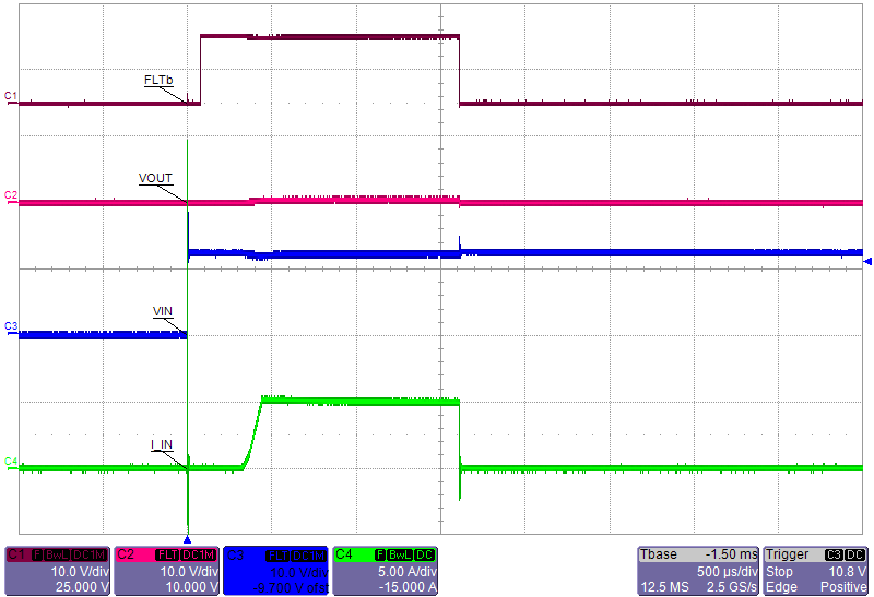 Figure 70. Hot Plug-In with Short on Output: Latched—TPS25942L
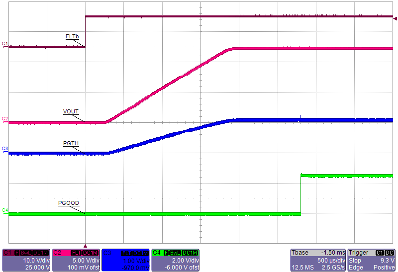 Figure 72. Power Good Response During Turnon
10.3 System Examples
The TPS25942 and TPS25944 provide a simple solution for power multiplexing applications through seamless transition between two power supplies, each operating at 2.7 V to 18 V and delivering up to 5 A. The devices with a distinctive feature set of true-reverse blocking, auto-forward conduction and fast switch over, support applications for both Active ORing and Priority power multiplexing.
10.3.1 Active ORing (Auto-Power Multiplexer) Operation
A typical redundant power supply configuration of the system is shown in Figure 74. Schottky ORing diodes have been popular for connecting parallel power supplies, such as parallel operation of wall adapter with a battery or a hold-up storage capacitor. The disadvantage of using ORing diodes is high voltage drop and associated power loss. The TPS25942 and TPS25944 with an integrated, low-ohmic N-channel FET provide a simple and efficient solution. Figure 74 shows the Active ORing implementation using the devices.
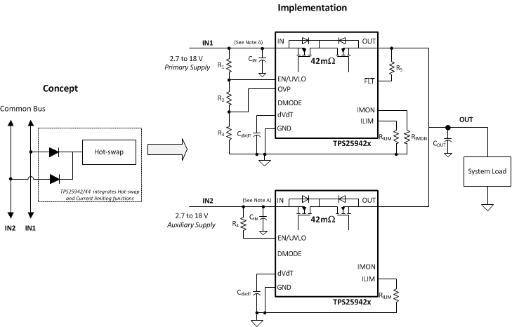
A fast reverse comparator controls the internal FET and it is turned ON or OFF with hysteresis as shown in Figure 75. The internal FET is turned ON in less than 4 us (typical) when the forward voltage drop V(IN) – V(OUT) exceeds 100 mV and is turned off in 1 µs (typical) as soon as V(IN) – V(OUT) falls below –10 mV. When internal FET is turned ON, the ORed input supply experiences momentary in-rush current drawn as the FET turns on charging the bus capacitance. In addition, device can be operated in Diode Mode by independently controlling DMODE pin.
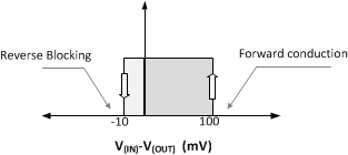 Figure 75. Active ORing Thresholds
Figure 75 shows typical switch-over waveforms of Active ORing implementation using the TPS25942 or TPS25944.
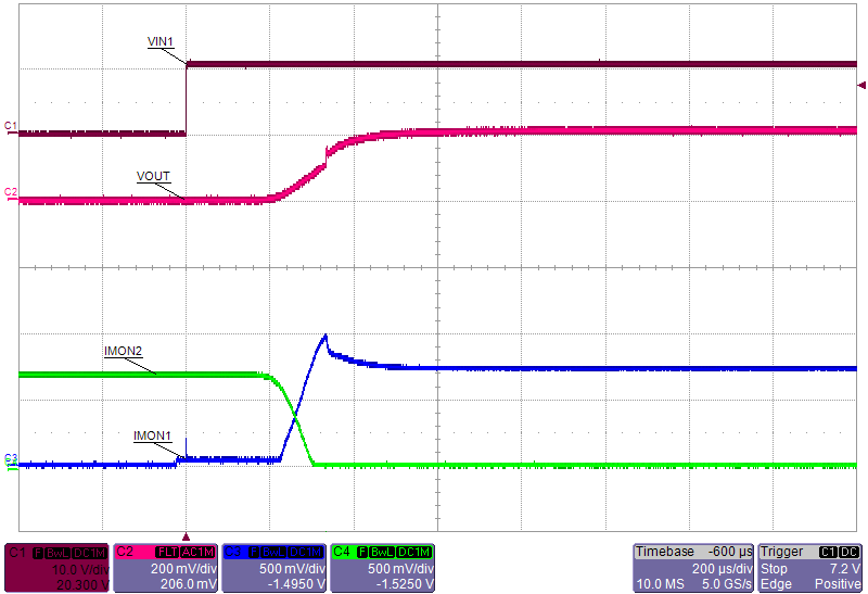
| V(IN1) = 12.2 V | V(IN2) = 12 V | C(OUT) = 100 µF |
| RL = 14 Ω | C(dVdT) = 1.5 nF |
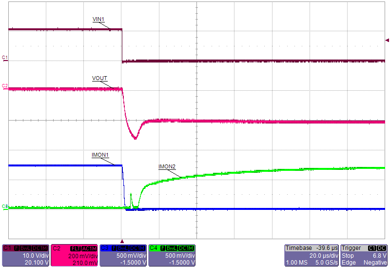
| V(IN1) = 12.2 V | V(IN2) = 12 V | C(OUT) = 100 µF |
| RL = 14 Ω | C(dVdT) = 1.5 nF |
When bus voltages (IN1 and IN2) are matched, device in each rail sees a forward voltage drop and is ON delivering the load current. During this period, current is shared between the rails in the ratio of differential voltage drop across each device.
In addition to above, the devices provide inrush current limit and protects each rail from potential overload and short circuit faults.
10.3.1.1 N+1 Power Supply Operation
The devices can be used to combine multiple power supplies to a common bus in an N+1 configuration. The N+1 power supply configuration as shown in Figure 78, is used where multiple power supplies are paralleled for either higher capacity, redundancy or both. If it takes N supplies to power the load, adding an extra identical unit in parallel permits the load to continue operation in the event that any one of the N supplies fails. The devices emulate the function of the ORing diode and provides with all protections as needed to isolate the rail during hot-plug, overvoltage, undervoltage, overcurrent and short-circuit conditions.
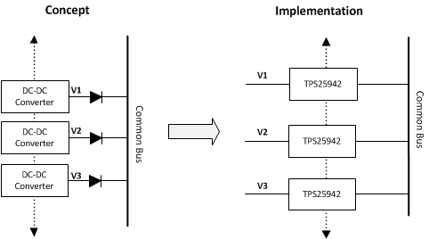 Figure 78. N+1 Configuration Implementation
10.3.1.2 Priority Power MUX Operation
Applications having two energy sources such as PCIe cards, Tablets and Portable battery powered equipment require preference of one source to another. For example, mains power (wall-adapter) has the priority over the internal back-up power or auxiliary power. These applications demand for switch over from mains power to back-up power only when main input voltage falls below a user defined threshold. The devices provide a simple solution for priority power multiplexing needs.
Figure 79 shows a typical priority power multiplexing implementation using devices. When primary power IN1 is present, the device in IN1 path powers the OUT bus irrespective of whether auxiliary power IN2 is greater than or less than IN1. Once the voltage on the IN1 rail falls below the user-defined threshold, the device IN1 issues a signal to switch over to auxiliary power IN2. The transition happens seamlessly in less than 125 µs, with minimal voltage droop on the bus. The voltage droop during transition is a function of load current and bus capacitance (see Equation 36).

where
- V(droop) in Volts, I(Load) is load current in Ampere, C(BUS) is bus capacitance in µF
When the main voltage supply (IN1) is not present or during brown-out conditions, the device in auxiliary supply rail (IN2) provides power to the output. When IN1 recovers, the device connected to IN1 is turned on at defined slew rate and the device in IN2 path is turned off, allowing a seamless transition from auxiliary to the main voltage supply with minimal droop and with no shoot-through current.
Priority power multiplexing can be done either between two similar rails (such as 12 V Primary to 12 V Aux, 3.3 V Primary to 3.3 V Aux) or between dissimilar rails (such as 12 V Primary to 5 V Aux or 3.3 V Aux; or vice versa).
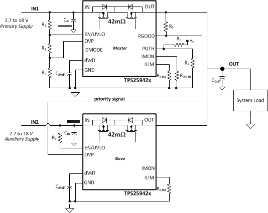
Figure 80 and Figure 81 show typical switch-over waveforms of Priority Muxing implementation using the TPS25942 or TPS25944 for 11.5 V Primary and 14.5 V Auxiliary Bus.
Figure 82 and Figure 83 show typical switch-over waveforms of Priority Muxing implementation using the TPS25942 or TPS25944 for 12 V Primary and 3.3 V Auxiliary Bus.
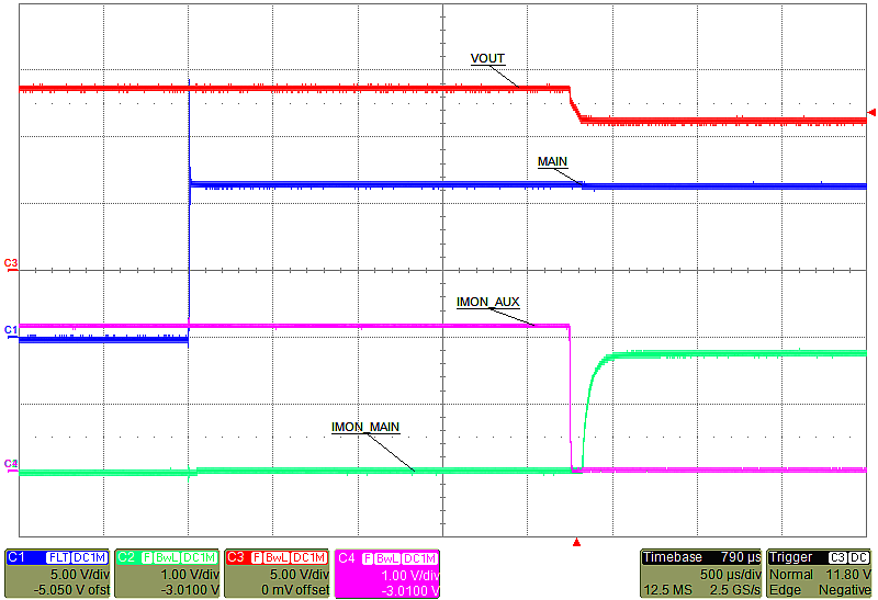
| V(IN1) = 11.5 V | R(ILIM1) = 24.6 kΩ, | C(OUT) = 150 µF |
| V(IN2) = 14.5 V | R(ILIM2) = 33.2 kΩ | C(dVdT) = 1.2 nF |
| RL = 5.6 Ω | R(IMON) = 16.2 kΩ | V(UVLO-High) = 10.8 V |
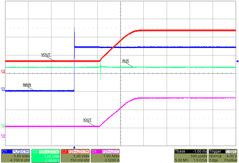
| V(IN1) = 12 V | R(ILIM1) = 24.6 kΩ | C(OUT) = 150 µF |
| V(IN2) = 3.3 V | R(ILIM2) = 33.2 kΩ | C(dVdT) = 1.2 nF |
| RLoad = 5.6 Ω | R(IMON) = 16.2 kΩ | V(UVLO-High) = 10.8 V |
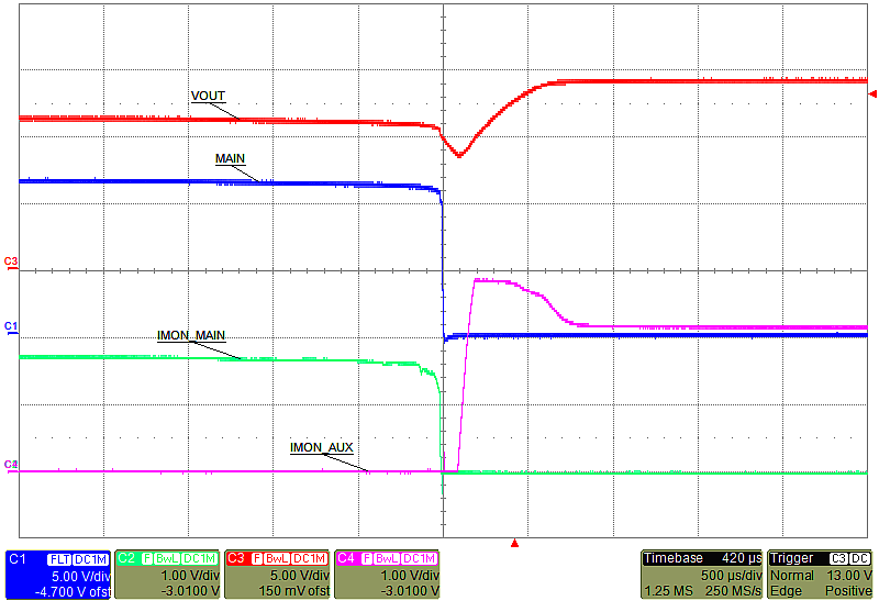
| V(IN1) = 11.5 V | R(ILIM1) = 24.6 kΩ | C(OUT) = 150 µF |
| V(IN2) = 14.5 V | R(ILIM2) = 33.2 kΩ | C(dVdT) = 1.2 nF |
| RL = 5.6 Ω | R(IMON) = 16.2 kΩ | V(UVLO-Low) = 10.2 V |
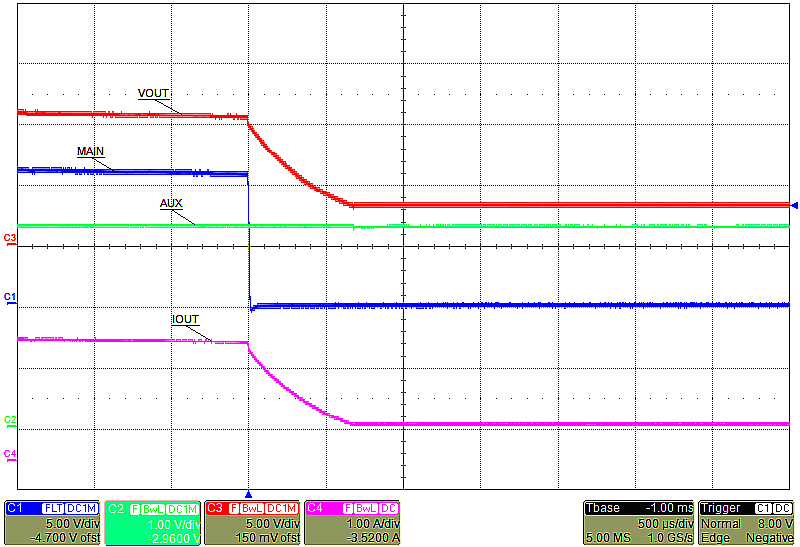
| V(IN1) = 12 V | R(ILIM1) = 24.6 kΩ | C(OUT) = 150 µF |
| V(IN2) = 3.3 V | R(ILIM2) = 33.2 kΩ | C(dVdT) = 1.2 nF |
| RL = 5.6 Ω | R(IMON) = 16.2 kΩ | V(UVLO-Low) = 10.2 V |
10.3.1.3 Priority MUXing With Almost Equal Rails (VIN1 ~ VIN2)
Most of the redundant power supply systems used in servers, storage and telecom, multiplex tightly regulated power rails to provide uninterrupted power to the load. In these systems, the primary and auxiliary rails are close to each other, typically within one diode drop when both rails are active.
For priority multiplexing in these systems, the TPS25942 or TPS25944 device in auxiliary rail path can be operated in Diode Mode for a fast switch-over (1 µs typical). The fast switch-over reduces the required hold-up capacitor on the output rail for a given droop specification.
The circuit implementation of this configuration is shown in Figure 84. During power-fail (brown-out) conditions of primary rail IN1, it changes IN2 from ‘Diode-Mode’ to normal operation using PGOOD. Similarly during power recovery of primary rail IN1, the auxiliary rail IN2 is driven into ‘Diode-Mode’.
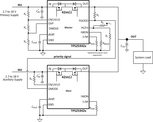 Figure 84. Priority Power Multiplexing Configuration for Almost Equal Rails
The fast switch-over performance is shown in Figure 85.
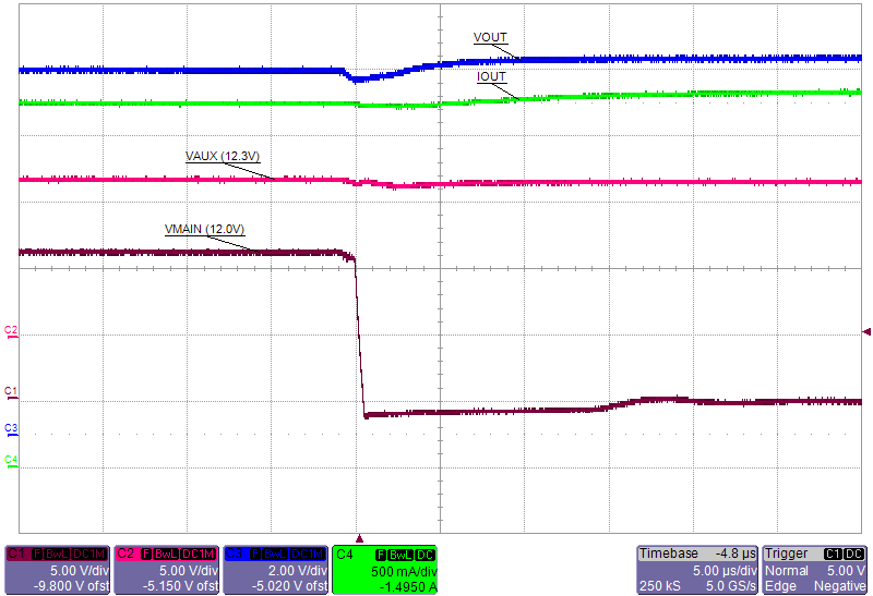
| C(OUT) = 150 µF | RL = 4 Ω |
10.3.1.4 Reverse Polarity Protection
In applications demanding reverse polarity or reverse battery protection, the TPS25942 and TPS25944 can be used as an eFuse or ideal diode. A typical reverse polarity protection circuitry is shown in Figure 86. The signal diode in the GND terminal path ensures that device is not functional during reverse polarity conditions and internal FET blocks the reverse path.
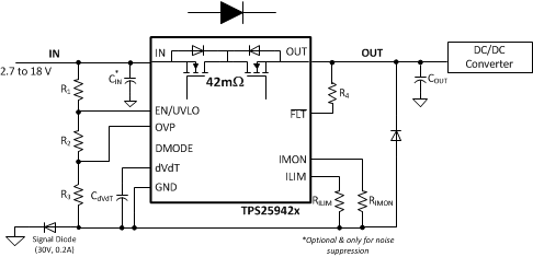 Figure 86. Reverse Polarity Protection Implementation