ZHCSCJ3D June 2014 – October 2017 TPS25942A , TPS25942L , TPS25944A , TPS25944L
UNLESS OTHERWISE NOTED, this document contains PRODUCTION DATA.
- 1 特性
- 2 应用范围
- 3 说明
- 4 修订历史记录
- 5 Device Comparison Table
- 6 Pin Configuration and Functions
- 7 Specifications
- 8 Parameter Measurement Information
-
9 Detailed Description
- 9.1 Overview
- 9.2 Functional Block Diagram
- 9.3
Feature Description
- 9.3.1 Enable and Adjusting Undervoltage Lockout
- 9.3.2 Overvoltage Protection (OVP)
- 9.3.3 Hot Plug-In and In-Rush Current Control
- 9.3.4 Overload and Short Circuit Protection
- 9.3.5 Reverse Current Protection
- 9.3.6 FAULT Response
- 9.3.7 Current Monitoring
- 9.3.8 Power Good Comparator
- 9.3.9 IN, OUT and GND Pins
- 9.3.10 Thermal Shutdown
- 9.4 Device Functional Modes
-
10Application and Implementation
- 10.1 Application Information
- 10.2
Typical Application
- 10.2.1 Design Requirements
- 10.2.2
Detailed Design Procedure
- 10.2.2.1 Step by Step Design Procedure
- 10.2.2.2 Programming the Current-Limit Threshold: R(ILIM) Selection
- 10.2.2.3 Undervoltage Lockout and Overvoltage Set Point
- 10.2.2.4 Programming Current Monitoring Resistor—RIMON
- 10.2.2.5 Setting Output Voltage Ramp Time (tdVdT)
- 10.2.2.6 Programing the Power Good Set Point
- 10.2.2.7 Support Component Selections—R6, R7 and CIN
- 10.2.3 Application Curves
- 10.3 System Examples
- 11Power Supply Recommendations
- 12Layout
- 13器件和文档支持
- 14机械、封装和可订购信息
12 Layout
12.1 Layout Guidelines
- For all applications, a 0.1-uF or greater ceramic decoupling capacitor is recommended between IN terminal and GND. For hot-plug applications, where input power path inductance is negligible, this capacitor can be eliminated or minimized.
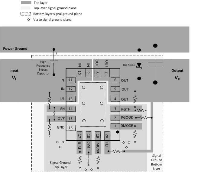
- The optimum placement of decoupling capacitor is closest to the IN and GND terminals of the device. Care must be taken to minimize the loop area formed by the bypass-capacitor connection, the IN terminal, and the GND terminal of the IC. See Figure 88 for a PCB layout example.
- High current carrying power path connections must be as short as possible and must be sized to carry at least twice the full-load current.
- Low current signal ground (SGND), which is the reference ground for the device must be a copper plane or island.
- Locate all the TPS25942, TPS25944 support components: R(ILIM), CdVdT, R(IMON), and resistors for UVLO and OVP, close to their connection pin. Connect the other end of the component to the SGND with shortest trace length.
- The trace routing for the RILIM and R(IMON) components to the device must be as short as possible to reduce parasitic effects on the current limit and current monitoring accuracy. These traces must not have any coupling to switching signals on the board.
- The SGND plane must be connected to high current ground (main power ground) at a single point, that is at the negative terminal of input capacitor.
- Protection devices such as TVS, snubbers, capacitors, or diodes must be placed physically close to the device they are intended to protect, and routed with short traces to reduce inductance. For example, a protection Schottky diode is recommended to address negative transients due to switching of inductive loads, and it must be physically close to the OUT pins.
- Thermal Considerations: When properly mounted the PowerPAD™ package provides significantly greater cooling ability than an ordinary package. To operate at rated power, the PowerPAD must be soldered directly to the board GND plane directly under the device. The PowerPAD is at GND potential and can be connected using multiple vias to inner layer GND. Other planes, such as the bottom side of the circuit board can be used to increase heat sinking in higher current applications. See the Technical Briefs: PowerPad™ Thermally Enhanced Package ( SLMA002) and PowerPAD™ Made Easy (SLMA004) for more information on using this PowerPAD™ package.
- The thermal via land pattern specific to the TPS25942, TPS25944 can be downloaded from device webpage.
- Obtaining acceptable performance with alternate layout schemes is possible; however this layout has been shown to produce good results and is intended as a guideline.
12.2 Layout Example

A. Optional: Needed only to suppress the transients caused by inductive load switching.
Figure 88. Board Layout