ZHCSL91B October 2020 – March 2022 TPS25947
PRODUCTION DATA
- 1 特性
- 2 应用
- 3 说明
- 4 Revision History
- 5 Device Comparison Table
- 6 Pin Configuration and Functions
- 7 Specifications
-
8 Detailed Description
- 8.1 Overview
- 8.2 Functional Block Diagram
- 8.3
Feature Description
- 8.3.1 Input Reverse Polarity Protection
- 8.3.2 Undervoltage Lockout (UVLO and UVP)
- 8.3.3 Overvoltage Lockout (OVLO)
- 8.3.4 Overvoltage Clamp (OVC)
- 8.3.5 Inrush Current, Overcurrent, and Short Circuit Protection
- 8.3.6 Analog Load Current Monitor
- 8.3.7 Reverse Current Protection
- 8.3.8 Overtemperature Protection (OTP)
- 8.3.9 Fault Response and Indication (FLT)
- 8.3.10 Auxiliary Channel Control (AUXOFF)
- 8.3.11 Power Good Indication (PG)
- 8.4 Device Functional Modes
- 9 Application and Implementation
- 10Power Supply Recommendations
- 11Layout
- 12Device and Documentation Support
- 13Mechanical, Packaging, and Orderable Information
8.3.7 Reverse Current Protection
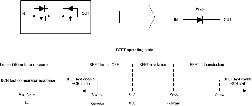
The device functions like an ideal diode and blocks reverse current flow from OUT to IN under all conditions. The device has integrated back-to-back MOSFETs connected in a common drain configuration. The voltage drop between the IN and OUT pins is constantly monitored and the gate drive of the blocking FET (BFET) is adjusted as needed to regulate the forward voltage drop at VFWD. This closed loop regulation scheme (linear ORing control) enables graceful turn off of the MOSFET during a reverse current event and ensures there is no DC reverse current flow.
The device also uses a conventional comparator (VREVTH) based reverse blocking mechanism to provide fast response (tRCB) to transient reverse currents. After the device enters reverse current blocking condition, it waits for the (VIN – VOUT) forward drop to exceed the VFWDTH before it performs a fast recovery to reach full forward conduction state. This provides sufficient hysterisis to prevent supply noise or ripple from affecting the reverse current blocking response. The recovery from reverse current blocking is very fast (tSWRCB). This ensures minimum supply droop which is helpful in applications such as supply MUXing/ORing and USB Fast Role Swap (FRS).
 Figure 8-13 Reverse Current Blocking Response
The waveforms below illustrate the reverse current blocking performance in various scenarios.
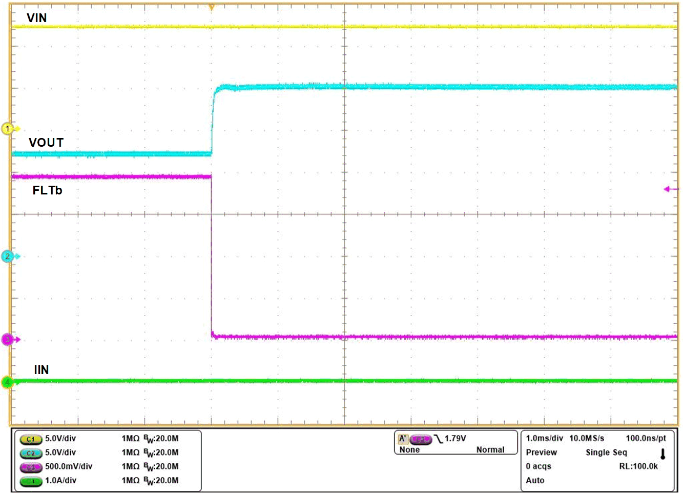
During fast voltage step at output (for example. hot-plug), the fast comparator based reverse blocking mechanism ensures minimum jump/glitch on the input rail.
 Figure 8-14 Reverse Current Blocking Performance During Fast Voltage Step at Output
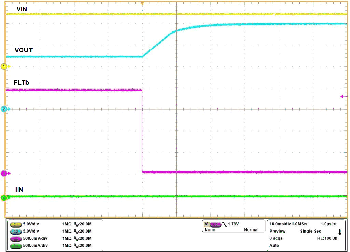
During slow voltage ramp at output, the linear ORing based reverse blocking mechanism ensures there is no DC current flow from OUT to IN, thereby avoiding input rail from getting slowly charged up to output voltage.
 Figure 8-15 Reverse Current Blocking Performance During Slow Voltage Ramp at Output
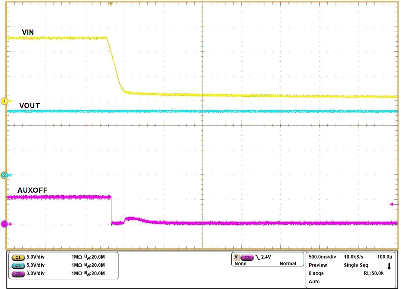
When the input supply droops or gets disconnected while the output storage element (bulk capacitor or super capacitor) is charged to the full voltage, the linear ORing scheme minimizes the self-discharge from OUT to IN. This ensures maximum hold-up time for the output storage element in critical power back-up applications.
It also prevents incorrect supply presence indication in applications which sense the input voltage to detect if the supply is connected.
 Figure 8-16 Reverse Current Blocking Performance During Input Supply Failure