ZHCSL91B October 2020 – March 2022 TPS25947
PRODUCTION DATA
- 1 特性
- 2 应用
- 3 说明
- 4 Revision History
- 5 Device Comparison Table
- 6 Pin Configuration and Functions
- 7 Specifications
-
8 Detailed Description
- 8.1 Overview
- 8.2 Functional Block Diagram
- 8.3
Feature Description
- 8.3.1 Input Reverse Polarity Protection
- 8.3.2 Undervoltage Lockout (UVLO and UVP)
- 8.3.3 Overvoltage Lockout (OVLO)
- 8.3.4 Overvoltage Clamp (OVC)
- 8.3.5 Inrush Current, Overcurrent, and Short Circuit Protection
- 8.3.6 Analog Load Current Monitor
- 8.3.7 Reverse Current Protection
- 8.3.8 Overtemperature Protection (OTP)
- 8.3.9 Fault Response and Indication (FLT)
- 8.3.10 Auxiliary Channel Control (AUXOFF)
- 8.3.11 Power Good Indication (PG)
- 8.4 Device Functional Modes
- 9 Application and Implementation
- 10Power Supply Recommendations
- 11Layout
- 12Device and Documentation Support
- 13Mechanical, Packaging, and Orderable Information
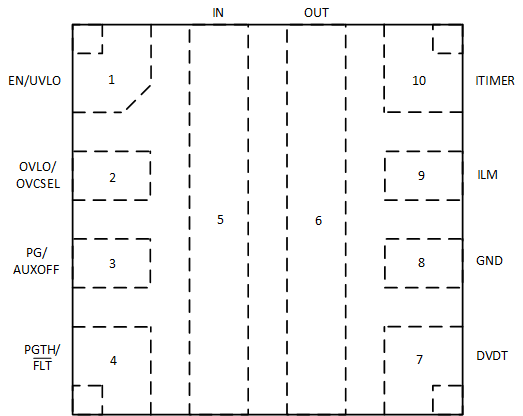
6 Pin Configuration and Functions
 Figure 6-1 TPS25947xx RPW Package 10-Pin QFN Top
View
Figure 6-1 TPS25947xx RPW Package 10-Pin QFN Top
ViewTable 6-1 Pin Functions
| PIN | TYPE | DESCRIPTION | |
|---|---|---|---|
| NAME | NO. | ||
| EN/UVLO |
1 | Analog Input | Active High Enable for the device. A Resistor Divider on this pin from input supply to GND can be used to adjust the Undervoltage Lockout threshold. Do not leave floating. Refer to Section 8.3.2 for details. |
|
OVLO |
2 | Analog Input | TPS259470x, TPS259474x: A Resistor Divider on this pin from supply to GND can be used to adjust the Overvoltage Lockout threshold. This pin can also be used as an Active Low Enable for the device. Do not leave floating. Refer to Section 8.3.3 for details. |
|
OVCSEL | Analog Input | TPS259472x: Overvoltage Clamp Threshold Select Pin. Refer to Section 8.3.4 for details. | |
|
PG |
3 | Digital Output | TPS259472x, TPS259474x: Power Good indication. This pin is an Open Drain signal which is asserted High when the internal powerpath is fully turned ON and PGTH input exceeds a certain threshold. Refer to Section 8.3.11 for more details. |
|
AUXOFF | Digital Output | TPS259470x: Auxiliary channel control signal. This pin is an Open Drain signal which is asserted High when the input supply is valid and channel has completed inrush sequence. This can be used to enable/disable the auxiliary supply eFuse to facilitate smooth switchover in a Priority power MUXing configuration. Refer to Section 8.3.10 for more details. | |
|
FLT |
4 | Digital Output | TPS259470x: Active low Fault event indicator. This pin is an Open Drain signal which will be pulled low when a fault is detected. Refer to Section 8.3.9 for more details. |
|
PGTH | Analog Input | TPS259472x, TPS259474x: Power Good Threshold. Refer to Section 8.3.11 for more details. | |
|
IN |
5 |
Power | Power input |
|
OUT |
6 |
Power | Power output |
|
DVDT |
7 | Analog Output | A capacitor from this pin to GND sets the output turn on slew rate. Leave this pin floating for the fastest turn on slew rate. Refer to Section 8.3.5.1 for details. |
|
GND |
8 |
Ground | This pin is the ground reference for all internal circuits and must be connected to system GND. |
|
ILM |
9 | Analog Output | This pin is a dual function pin used to limit and monitor the output current. An external resistor from this pin to GND sets the output current limit threshold during start-up as well as steady state. The pin voltage can also be used as analog output load current monitor signal. Do not leave floating. Refer to Section 8.3.5.2 or Section 8.3.5.3 for more details. |
|
ITIMER |
10 | Analog Output | A capacitor from this pin to GND sets the overcurrent blanking interval during which the output current can temporarily exceed set current limit (but lower than fast-trip threshold) before the device overcurrent response takes action. Leave this pin open for fastest response to overcurrent events. Refer to Section 8.3.5.2 or Section 8.3.5.3 for more details. |