ZHCSHV0C June 2017 – April 2018 TPS2595
PRODUCTION DATA.
- 1 特性
- 2 应用
- 3 说明
- 4 修订历史记录
- 5 Device Comparison Table
- 6 Pin Configuration and Functions
- 7 Specifications
-
8 Detailed Description
- 8.1 Overview
- 8.2 Functional Block Diagram
- 8.3 Feature Description
- 8.4 Device Functional Modes
-
9 Application and Implementation
- 9.1 Application Information
- 9.2
Typical Application
- 9.2.1 Design Requirements
- 9.2.2 Detailed Design Procedure
- 9.2.3 Support Component Selection: CIN
- 9.2.4 Application Curves
- 9.2.5 Controlled Power Down (Quick Output Discharge) using TPS2595x5
- 9.2.6 Overvoltage Lockout using TPS259573
- 10Power Supply Recommendations
- 11Layout
- 12器件和文档支持
- 13机械、封装和可订购信息
8.3.2.2 Overvoltage Clamp (OVC)
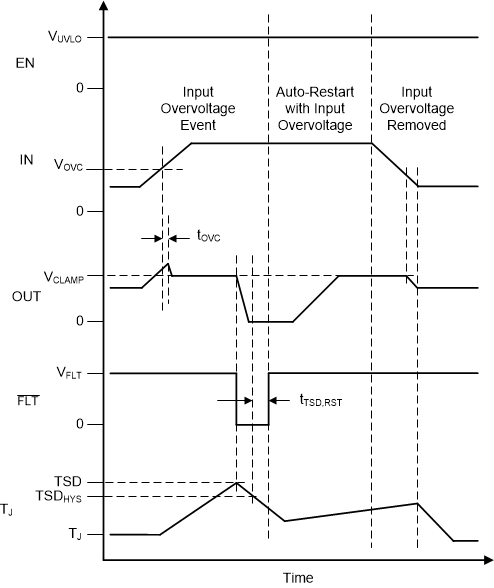
The TPS25952x, TPS25953x, TPS25954x devices provide a mechanism to clamp the output voltage to a predefined level quickly if the input voltage crosses a certain threshold. This ensures the load is not exposed to high voltages on any overvoltage at the input supply, and lowers the dependency on external protection devices (such as TVS/Zener diodes) in this condition. Once the input supply voltage rises above the OVC threshold voltage VOVC, the device responds by clamping the voltage to VCLAMP within a very short response time tOVC. As long as an overvoltage condition is present on the input, the output voltage will be clamped to VCLAMP. When the input drops below the output clamp threshold VOVC, the clamp releases the output voltage. See Figure 49.
During the overvoltage clamp condition, there could be significant heat dissipation in the internal FET depending on the VIN - VOUT voltage drop and the current through the FET leading to a thermal shutdown if the condition persists for an extended period of time. In this case, the device would either stay latched-off or start a auto retry cycle as explained in the Overtemperature Protection (OTP) section.
 Figure 49. TPS2595xx Overvoltage Clamp Response (Auto-Retry)
Multiple device options are offered with different clamping voltage thresholds. See the Device Comparison Table for list of available voltage clamp options.