ZHCSHV0C June 2017 – April 2018 TPS2595
PRODUCTION DATA.
- 1 特性
- 2 应用
- 3 说明
- 4 修订历史记录
- 5 Device Comparison Table
- 6 Pin Configuration and Functions
- 7 Specifications
-
8 Detailed Description
- 8.1 Overview
- 8.2 Functional Block Diagram
- 8.3 Feature Description
- 8.4 Device Functional Modes
-
9 Application and Implementation
- 9.1 Application Information
- 9.2
Typical Application
- 9.2.1 Design Requirements
- 9.2.2 Detailed Design Procedure
- 9.2.3 Support Component Selection: CIN
- 9.2.4 Application Curves
- 9.2.5 Controlled Power Down (Quick Output Discharge) using TPS2595x5
- 9.2.6 Overvoltage Lockout using TPS259573
- 10Power Supply Recommendations
- 11Layout
- 12器件和文档支持
- 13机械、封装和可订购信息
6 Pin Configuration and Functions
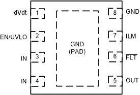
TPS2595x0/1 DSG Package
8-Pin WSON
Top View

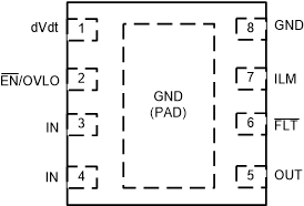
TPS2595x3 DSG Package
8-Pin WSON
Top View

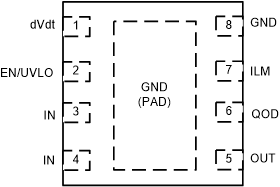
TPS2595x5 DSG Package
8-Pin WSON
Top View

Pin Functions
| PIN | TYPE | DESCRIPTION | |
|---|---|---|---|
| NO. | NAME | ||
| 1 | dVdt | Analog I/O | A capacitor from this pin to GND sets the output turn on slew rate. Leave this pin floating for the fastest turn on slew rate. (See Switching Characteristics). |
| 2 | EN/UVLO | Analog input | Active high enable for the TPS2595x0, TPS2595x1, TPS2595x5 variants. A resistor divider can be used to adjust the undervoltage lockout threshold. Do not leave floating. |
| EN/OVLO | Active low enable for the TPS2595x3 variants. A resistor divider can be used to adjust the overvoltage lockout threshold. Do not leave floating. | ||
| 3,4 | IN | Power | Power input |
| 5 | OUT | Power | Power output |
| 6 | FLT | Digital output | TPS2595x0, TPS2595x1, TPS2595x3: Fault event indicator which is pulled low when a fault is detected. It is an open drain output that requires an external pull up resistance. |
| QOD | TPS2595x5: Quick Output Discharge Pin, when tied to OUT directly or through external resistor. | ||
| 7 | ILM | Analog I/O | This is a dual function pin used to limit and monitor the output current. An external resistor from this pin to GND sets the output current limit. The pin voltage can also be used to monitor the output load current. Do not leave floating. |
| 8 | GND | Ground | Ground |
| PAD | GND | Thermal/Ground | The exposed pad is used primarily for heat dissipation and must be connected to GND. |