ZHCSJQ2A May 2019 – August 2019 TPS2596
PRODUCTION DATA.
- 1 特性
- 2 应用
- 3 说明
- 4 修订历史记录
- 5 器件比较表
- 6 Pin Configuration and Functions
- 7 Specifications
-
8 Detailed Description
- 8.1 Overview
- 8.2 Functional Block Diagram
- 8.3 Feature Description
- 8.4 Device Functional Modes
-
9 Application and Implementation
- 9.1 Application Information
- 9.2
Typical Application
- 9.2.1 Precision Current Limiting and Protection for White Goods
- 9.2.2 Design Requirements
- 9.2.3 Detailed Design Procedure
- 9.2.4 Support Component Selection: RFLT and CIN
- 9.2.5 Application Curves
- 9.3 System Examples
- 10Power Supply Recommendations
- 11Layout
- 12器件和文档支持
- 13机械、封装和可订购信息
8.3.2.2 Overvoltage Clamp
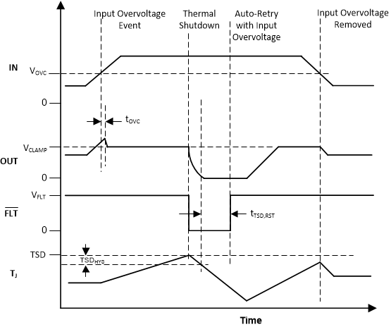
The TPS25962x variants provide a mechanism to clamp the output voltage to a user-selectable level quickly if the input voltage crosses a certain threshold. This ensures the load is not exposed to high voltages during any input overvoltage events and lowers the dependence on external protection devices (such as TVS/Zener diodes) in this condition. Once the input supply voltage rises above the OVC threshold voltage VOVC, the device responds by clamping the voltage to VCLAMP within a very short response time tOVC. As long as an overvoltage condition is present on the input, the output voltage will be clamped to VCLAMP. When the input drops below the output clamp threshold VOVC, the clamp releases the output voltage as shown in Figure 47.
 Figure 47. TPS25962x Overvoltage Clamp Response
 The OVC threshold can be configured to one of 3 pre-defined levels by connecting the OVCSEL pin as shown in Table 1.
Table 1. TPS25962x Overvoltage Clamp Threshold Selection
| OVCSEL Pin Connection | OVC Threshold (typ) |
|---|---|
| Shorted to GND | 3.8 V |
| Connected to GND through 400 KΩ resistor | 5.7 V |
| Open | 13.7 V |
During the overvoltage clamp condition, there could be significant heat dissipation in the internal FET depending on the VIN - VOUT voltage drop and the current (IOUT) through the FET leading to thermal shutdown if the condition persists for an extended period of time. In this case, the device would either stay latched-off or start an auto-retry cycle as explained in the Overtemperature Protection (OTP) section.