ZHCSJQ2A May 2019 – August 2019 TPS2596
PRODUCTION DATA.
- 1 特性
- 2 应用
- 3 说明
- 4 修订历史记录
- 5 器件比较表
- 6 Pin Configuration and Functions
- 7 Specifications
-
8 Detailed Description
- 8.1 Overview
- 8.2 Functional Block Diagram
- 8.3 Feature Description
- 8.4 Device Functional Modes
-
9 Application and Implementation
- 9.1 Application Information
- 9.2
Typical Application
- 9.2.1 Precision Current Limiting and Protection for White Goods
- 9.2.2 Design Requirements
- 9.2.3 Detailed Design Procedure
- 9.2.4 Support Component Selection: RFLT and CIN
- 9.2.5 Application Curves
- 9.3 System Examples
- 10Power Supply Recommendations
- 11Layout
- 12器件和文档支持
- 13机械、封装和可订购信息
9.2.3.3.2 Case 2: Start-Up With Load. Output Capacitance COUT and Load Draw Current
When the load draws current during the turnon sequence, there is additional power dissipated. Considering a resistive load during start-up RL(SU), load current ramps up proportionally with increase in output voltage during TdVdT time. Equations 12 to 15 show the average power dissipation in the internal FET during charging time due to resistive load.

Total power dissipated in the device during start-up is Equation 13.

Total current during start-up is given by Equation 14.

If ISTARTUP > ILIMIT, the device limits the current to ILIMIT and the current-limited charging time is determined by Equation 15.

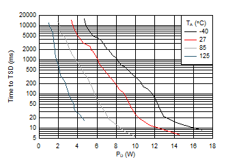
The power dissipation, with and without load, for selected start-up time must not exceed the shutdown limits as shown in Figure 55.
 Figure 55. Thermal Shutdown Limit Plot
 For the design example under discussion, select ramp-up capacitor CdVdt = 22000 pF. The default slew rate for CdVdt = 22000 pF is 1.9 mV/µs. With slew rate of 1.9 mV/µs, the ramp-up time TdVdt for 12 V input is 6.3 ms.
The inrush current drawn by the load capacitance COUT during ramp-up using Equation 16.

The inrush power dissipation is calculated using Equation 17.

For 1.14 W of power loss, the thermal shutdown time of the device must not be less than the ramp-up time TdVdt to avoid the false trip at the maximum operating temperature. Figure 55 shows the thermal shutdown limit at TA = 85 °C, for 1.14 W of power, the shutdown time is infinite. Therefore, it is safe to use 6.3 ms as the start-up time without any load on the output.
The additional power dissipation when a 10-Ω load is present during start-up is calculated using Equation 18.

The total device power dissipation during start-up is given in Equation 19.

Figure 55 shows TA = 85 °C and the thermal shutdown time for 2.24 W is approximately 2000 ms, which increases the margins further for shutdown time and ensures successful operation during start up and steady state conditions.
When COUT is large, there is a need to decrease the power dissipation during start-up. This can be done by increasing the value of the CdVdt capacitor.