ZHCSQ76 December   2022 TPS25961

PRODUCTION DATA  

  1. 特性
  2. 应用
  3. 说明
  4. Revision History
  5. Pin Configuration and Functions
  6. Specifications
    1. 6.1 Absolute Maximum Ratings
    2. 6.2 ESD Ratings
    3. 6.3 Recommended Operating Conditions
    4. 6.4 Thermal Information
    5. 6.5 Electrical Characteristics
    6. 6.6 Timing Requirements
    7. 6.7 Switching Characteristics
    8. 6.8 典型特性
  7. Detailed Description
    1. 7.1 Overview
    2. 7.2 Functional Block Diagram
    3. 7.3 Feature Description
      1. 7.3.1 欠压保护 (UVP) 和欠压锁定 (UVLO)
      2. 7.3.2 Overvoltage Protection
      3. 7.3.3 Inrush Current, Overcurrent and Short Circuit Protection
        1. 7.3.3.1 Slew Rate and Inrush Current Control (dVdt)
        2. 7.3.3.2 Active Current Limiting
        3. 7.3.3.3 Short-Circuit Protection
      4. 7.3.4 Overtemperature Protection (OTP)
      5. 7.3.5 Fault Response
    4. 7.4 Device Functional Modes
  8. Application and Implementation
    1. 8.1 Application Information
    2. 8.2 典型应用
      1. 8.2.1 Adapter input protection for set-top boxes
      2. 8.2.2 Design Requirements
      3. 8.2.3 Detailed Design Procedure
        1. 8.2.3.1 Programming the Current-Limit Threshold: RILM Selection
        2. 8.2.3.2 欠压和过压锁定设定点
        3. 8.2.3.3 Output Voltage Rise Time (tR)
      4. 8.2.4 Application Curves
    3. 8.3 Application Example
      1. 8.3.1 Application Curves
    4. 8.4 Power Supply Recommendations
      1. 8.4.1 瞬态保护
      2. 8.4.2 Output Short-Circuit Measurements
    5. 8.5 Layout
      1. 8.5.1 Layout Guidelines
      2. 8.5.2 Layout Example
  9. Device and Documentation Support
    1. 9.1 Documentation Support
      1. 9.1.1 Related Documentation
    2. 9.2 接收文档更新通知
    3. 9.3 支持资源
    4. 9.4 商标
    5. 9.5 Electrostatic Discharge Caution
    6. 9.6 术语表
  10. 10Mechanical, Packaging, and Orderable Information

封装选项

机械数据 (封装 | 引脚)
散热焊盘机械数据 (封装 | 引脚)
订购信息

Pin Configuration and Functions

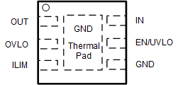
GUID-20220623-SS0I-TJKL-R1BC-Q2K9FGKLCXPS-low.gifFigure 5-1 DRV Package, 6-Pin SON(Top View)
Table 5-1 Pin Functions
PINI/ODESCRIPTION
NAMENO.
OUT1

Power

Power output.
OVLO2Analog InputAn external resistor divider from supply rail can be used to adjust the overvoltage lockout threshold. Connect to GND directly to use internal fixed overvoltage lockout threshold. Do not leave floating.

ILIM

3

Analog OutputAn external resistor from this pin to GND sets the output current limit threshold. Leave it open to set the current limit threshold to minimum value.

GND

4

Ground

Connect to system electrical ground.
EN/UVLO

5

Analog InputActive High Enable for the device. A resistor divider from supply rail can be used to adjust the undervoltage lockout threshold. Do not leave floating.
IN

6

PowerPower input.

GND

PAD

Thermal/Ground

The exposed pad is used primarily for heat dissipation and must be connected to GND plane on the PCB.