ZHCSOF8C november 2021 – april 2023 TPS2597
PRODUCTION DATA
- 1 特性
- 2 应用
- 3 说明
- 4 Revision History
- 5 Device Comparison Table
- 6 Pin Configuration and Functions
- 7 Specifications
-
8 Detailed Description
- 8.1 Overview
- 8.2 Functional Block Diagram
- 8.3
Feature Description
- 8.3.1 Undervoltage Lockout (UVLO and UVP)
- 8.3.2 Overvoltage Lockout (OVLO)
- 8.3.3 Overvoltage Clamp (OVC)
- 8.3.4 Inrush Current, Overcurrent, and Short Circuit Protection
- 8.3.5 Analog Load Current Monitor
- 8.3.6 Overtemperature Protection (OTP)
- 8.3.7 Fault Response and Indication (FLT)
- 8.3.8 Power-Good Indication (PG)
- 8.4 Device Functional Modes
- 9 Application and Implementation
- 10Device and Documentation Support
- 11Mechanical, Packaging, and Orderable Information
8.3.3 Overvoltage Clamp (OVC)
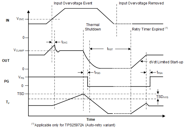
The TPS25972x variants implement a voltage clamp on the output to protect the system in the event of input overvoltage. When the device detects the input has exceeded the overvoltage clamp threshold (VOVC), it quickly responds within tOVC and stops the output from rising further. the device then regulates the HFET linearly to clamp the output voltage below VCLAMP as long as an overvoltage condition is present on the input.
If the part stays in clamping state for an extended period of time, there is higher power dissipation inside the part which can eventually lead to thermal shutdown (TSD). After the part shuts down due to TSD fault, it either stays latched off (TPS25972L variant) or restart automatically after a fixed delay (TPS25972A variant). See Overtemperature Protection (OTP) for more details on device response to overtemperature.
 Figure 8-8 TPS25972x Overvoltage Response (Auto-Retry)
There are three available overvoltage clamp threshold options, which can be configured using the OVCSEL pin.
| OVCSEL PIN CONNECTION | OVERVOLTAGE CLAMP THRESHOLD |
|---|---|
| Shorted to GND | 3.89 V |
| Open | 5.76 V |
| Connected to GND through a 390-kΩ resistor | 13.88 V |