ZHCSOF8C november 2021 – april 2023 TPS2597
PRODUCTION DATA
- 1 特性
- 2 应用
- 3 说明
- 4 Revision History
- 5 Device Comparison Table
- 6 Pin Configuration and Functions
- 7 Specifications
-
8 Detailed Description
- 8.1 Overview
- 8.2 Functional Block Diagram
- 8.3
Feature Description
- 8.3.1 Undervoltage Lockout (UVLO and UVP)
- 8.3.2 Overvoltage Lockout (OVLO)
- 8.3.3 Overvoltage Clamp (OVC)
- 8.3.4 Inrush Current, Overcurrent, and Short Circuit Protection
- 8.3.5 Analog Load Current Monitor
- 8.3.6 Overtemperature Protection (OTP)
- 8.3.7 Fault Response and Indication (FLT)
- 8.3.8 Power-Good Indication (PG)
- 8.4 Device Functional Modes
- 9 Application and Implementation
- 10Device and Documentation Support
- 11Mechanical, Packaging, and Orderable Information
7.8 Typical Characteristics
 Figure 7-1 ON-Resistance vs Supply Voltage
 Figure 7-3 IN Quiescent Current vs Temperature (TPS25972x Variant)
 Figure 7-5 IN Shutdown Current vs Temperature
 Figure 7-7 EN/UVLO Rising Threshold vs Temperature
 Figure 7-9 EN/UVLO Shutdown Falling Threshold vs Temperature
 Figure 7-11 OVLO Falling Threshold vs Temperature
(TPS25970x, TPS25974x Variants)
 Figure 7-13 Overcurrent Threshold Accuracy (Across
Process, Voltage and Temperature)
 Figure 7-15 Scalable Fast-Trip Threshold: Current Limit
Threshold (ILIM) Ratio vs Temperature
 Figure 7-17 OVC Clamping Voltage (OVCSEL = 390 kΩ to GND) vs Load Current (TPS25972x Variant)
 Figure 7-19 OVC Clamping Voltage (OVCSEL = GND) vs Load Current (TPS25972x Variant)
 Figure 7-21 ITIMER Discharge Current vs Temperature
 Figure 7-23 ITIMER internal Pullup Voltage vs
Temperature
 Figure 7-25 PGTH Threshold (Rising) vs Temperature
(TPS25972x, TPS25974x Variants)
 Figure 7-27 FLT Pin Pulldown
Resistance vs Temperature
 Figure 7-29 Time to Thermal Shut-Down During Steady State
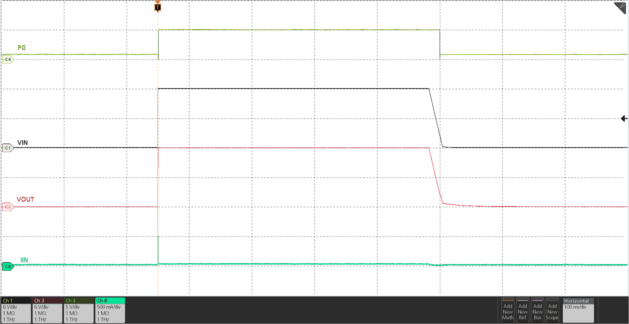
| VEN/UVLO = 2 V, COUT = 22 μF, CdVdt = Open, VIN ramped from 0 V → 12 V → 0 V |
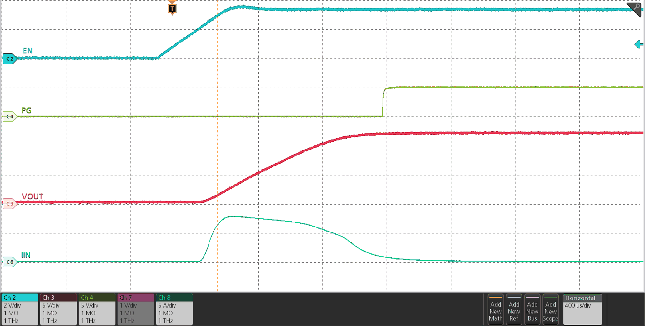
| VIN = 12 V, COUT = 470 μF, CdVdt = Open, VEN/UVLO stepped up to 3.3 V |
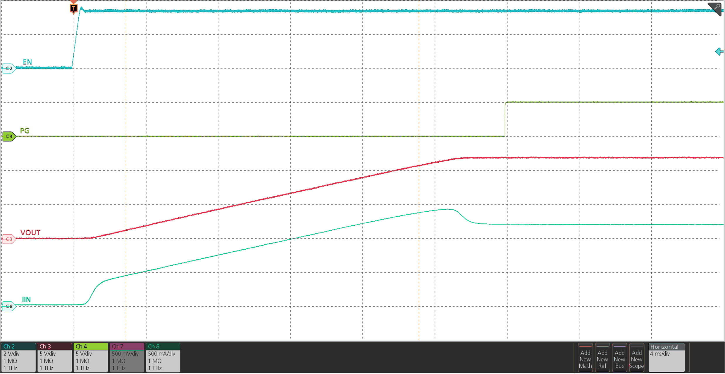
| VIN = 12 V, COUT = 470 μF, ROUT = 10 Ω, CdVdt = 5100 pF, VEN/UVLO stepped up to 3.3 V |
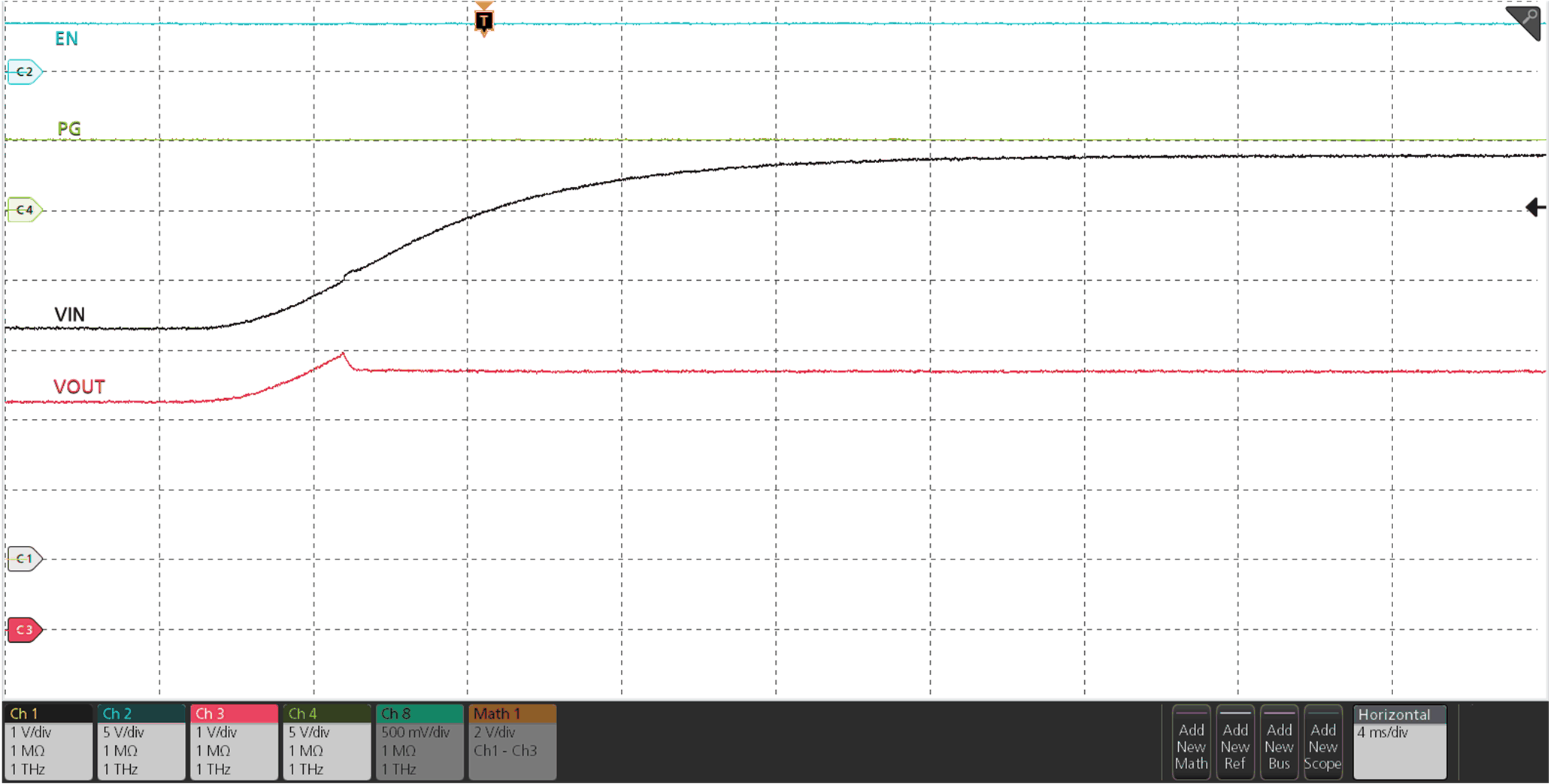
| ROVCSEL = GND, COUT = 220 μF, IOUT = 200 mA, VIN ramped up from 3.3 V to 5.8 V |
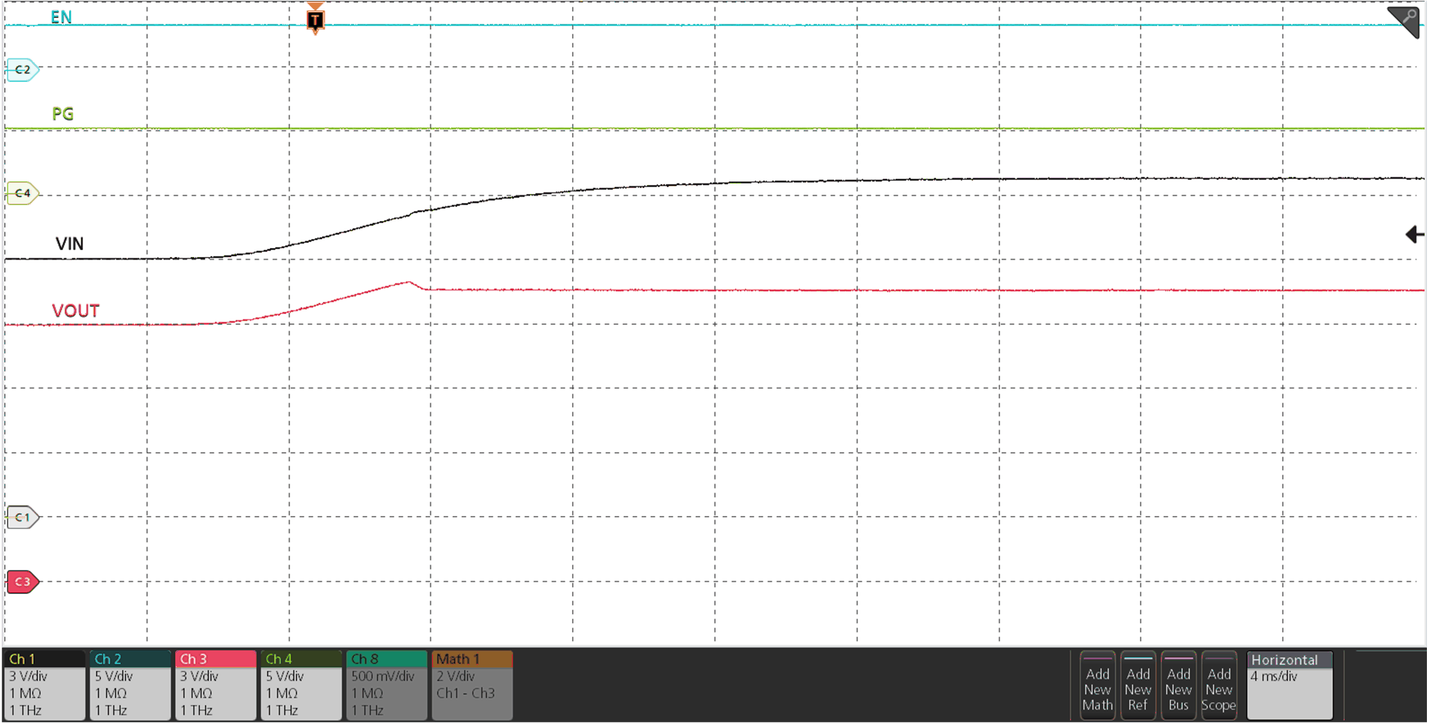
| ROVCSEL = 390 kΩ, COUT = 220 μF, IOUT = 200 mA, VIN ramped up from 12 V to 16.5 V |
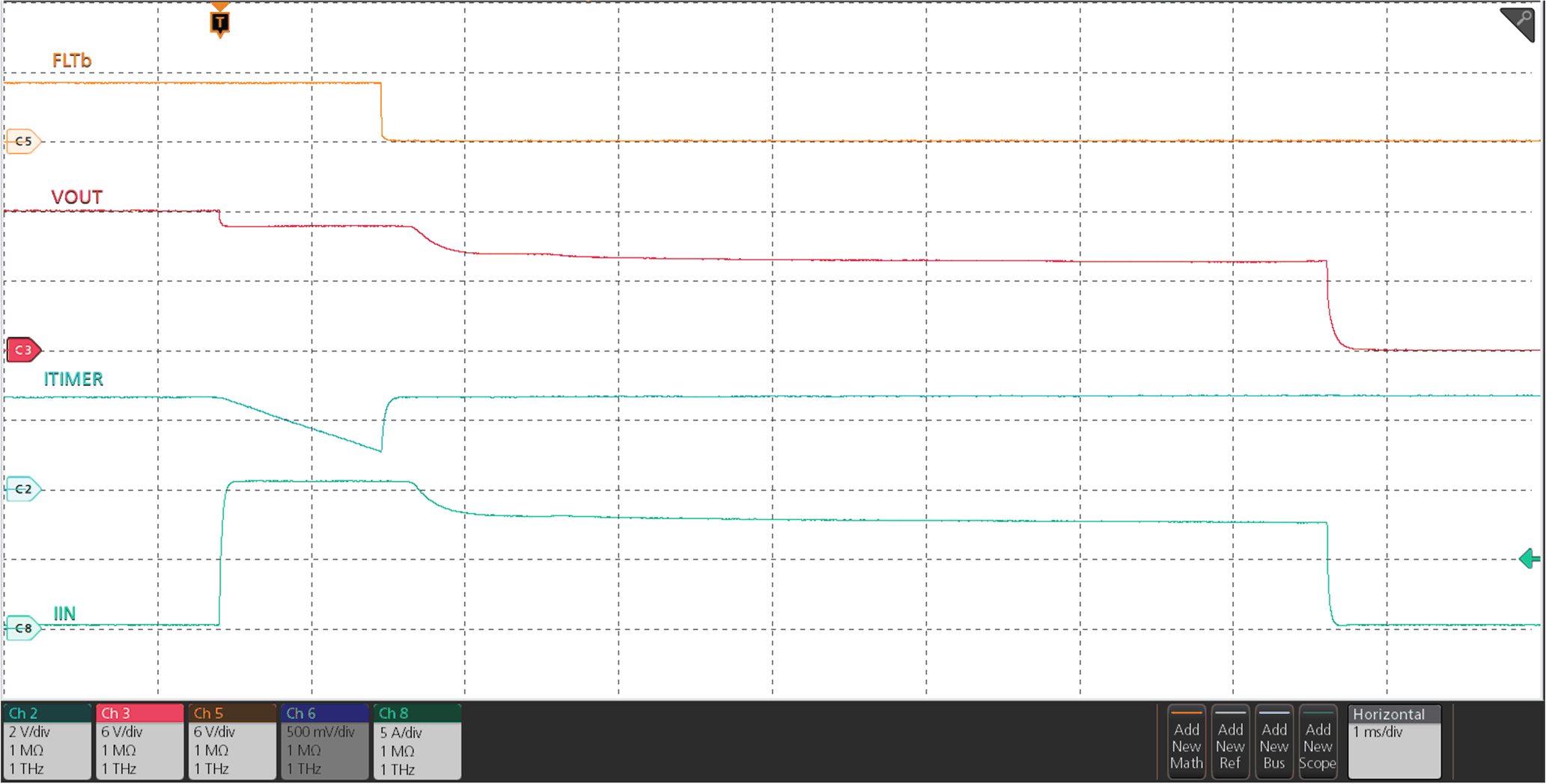
| VIN = 12 V, CITIMER = 1.3 nF, COUT = 220 μF, RILM = 715 Ω, IOUT stepped from 0 A → 11 A |
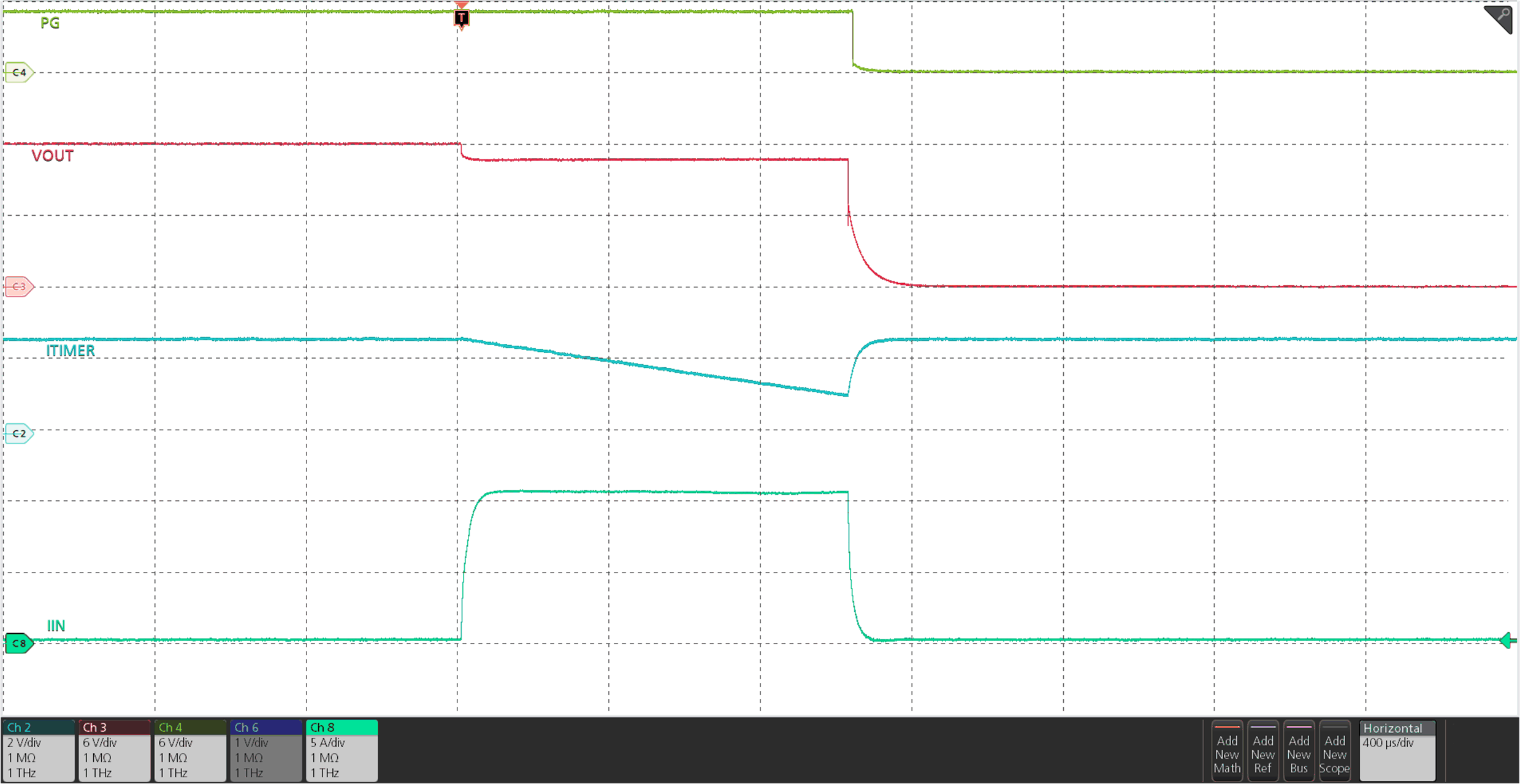
| VIN = 12 V, CITIMER = 1.3 nF, COUT = 470 μF, RILM = 715 Ω, IOUT stepped from 0 A → 11 A |
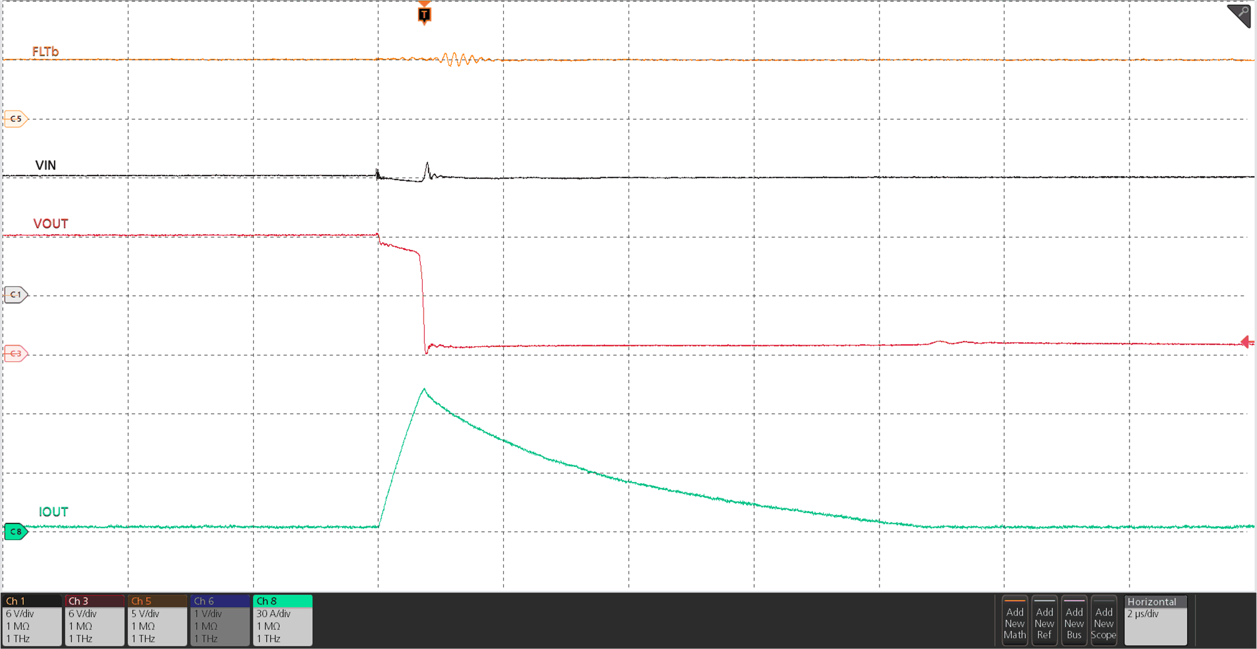
| VIN = 12 V, RILM = 715 Ω, OUT stepped from Open → Short-circuit to GND |
 Figure 7-2 IN Quiescent Current vs Temperature
(TPS25970x, TPS25974x Variants)
 Figure 7-4 IN OFF State (UVLO) Current vs
Temperature
 Figure 7-6 IN Undervoltage Threshold vs Temperature
 Figure 7-8 EN/UVLO Falling Threshold vs Temperature
 Figure 7-10 OVLO Rising Threshold vs Temperature
(TPS25970x, TPS25974x Variants)
 Figure 7-12 Overcurrent Threshold vs ILM Resistor
 Figure 7-14 Analog Current Monitor Gain Accuracy
 Figure 7-16 OVC Threshold vs Temperature (TPS25972x Variant)
 Figure 7-18 OVC Clamping Voltage (OVCSEL = OPEN) vs Load Current (TPS25972x Variant)
 Figure 7-20 ITIMER Discharge Differential Voltage
Threshold vs Temperature
 Figure 7-22 ITIMER Internal Pullup Resistance vs
Temperature
 Figure 7-24 DVDT Charging Current vs Temperature
 Figure 7-26 PGTH Threshold (Falling) vs Temperature
(TPS25972x, TPS25974x Variants)
 Figure 7-28 Time to Thermal Shut-Down During Inrush State
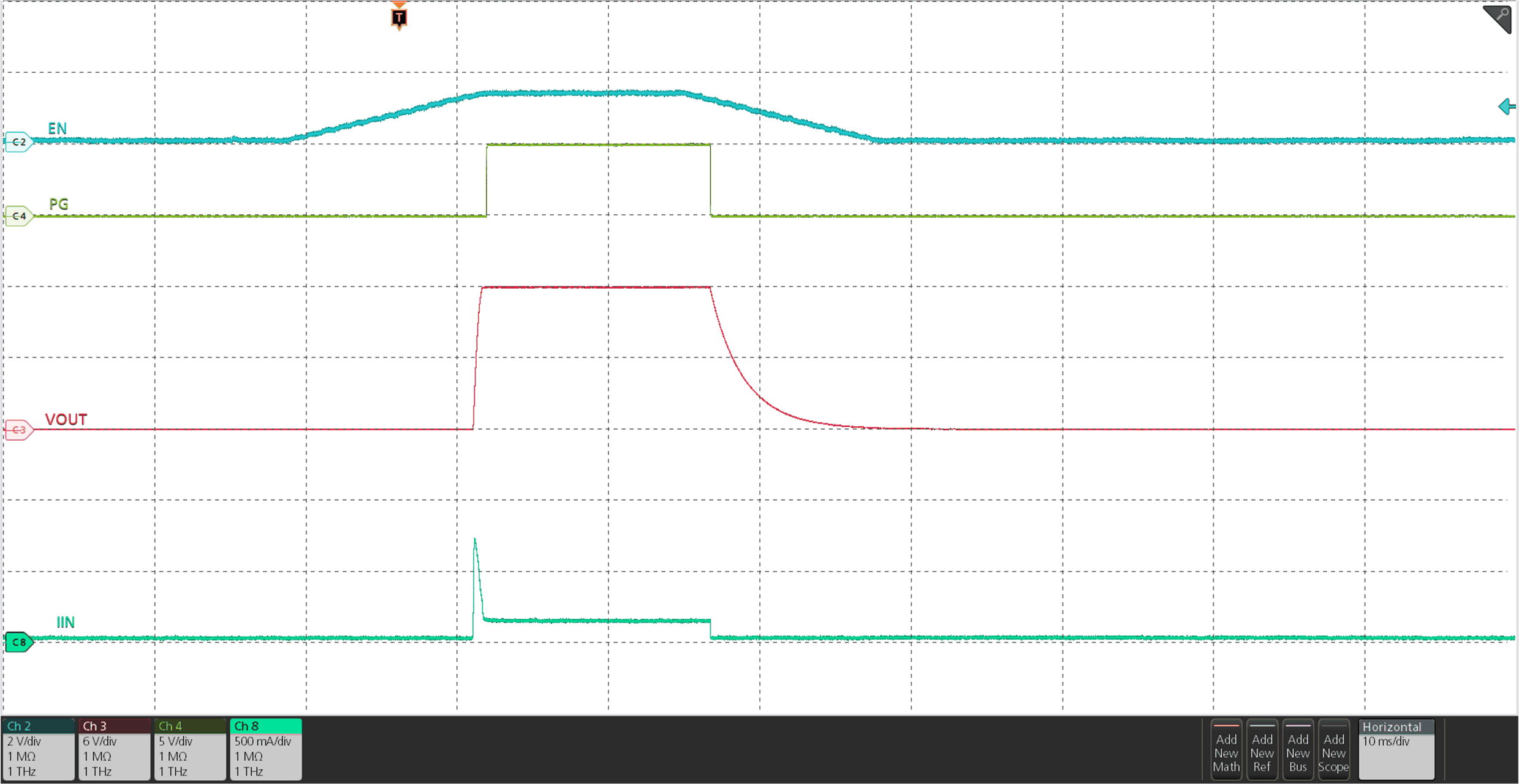
| VIN = 12 V, COUT = 22 μF, CdVdt = Open, VEN/UVLO ramped from 0 V → 1.4 V → 0 V |
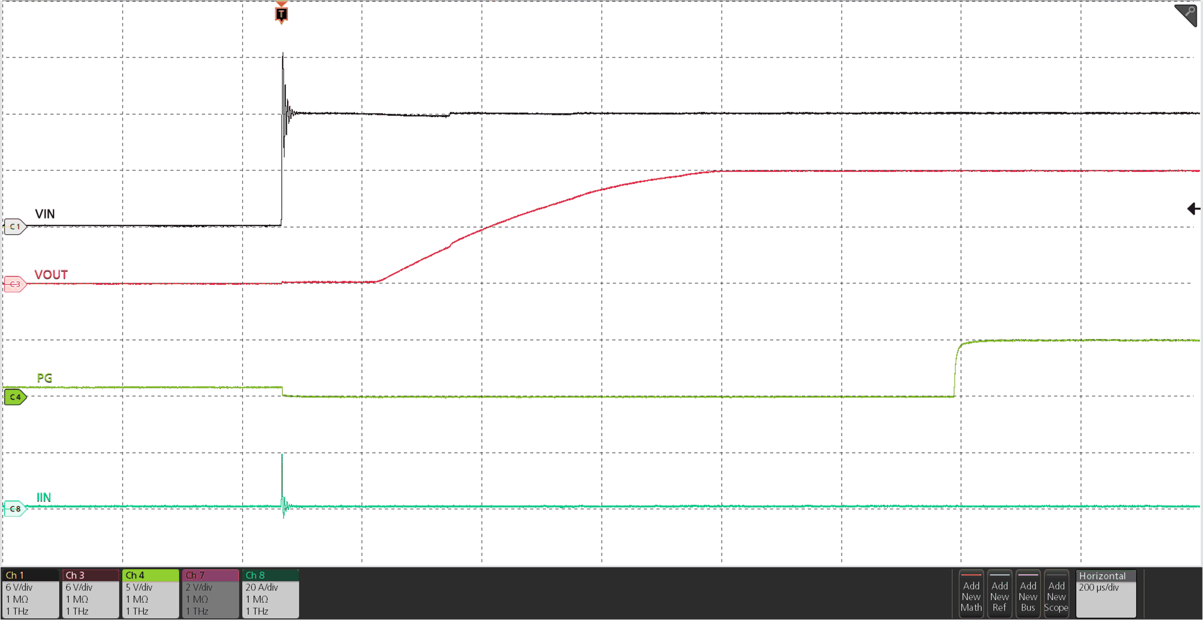
| COUT = 22 μF, CdVdt = Open, EN/UVLO connected to IN through resistor ladder, 12 V hot-plugged to IN |
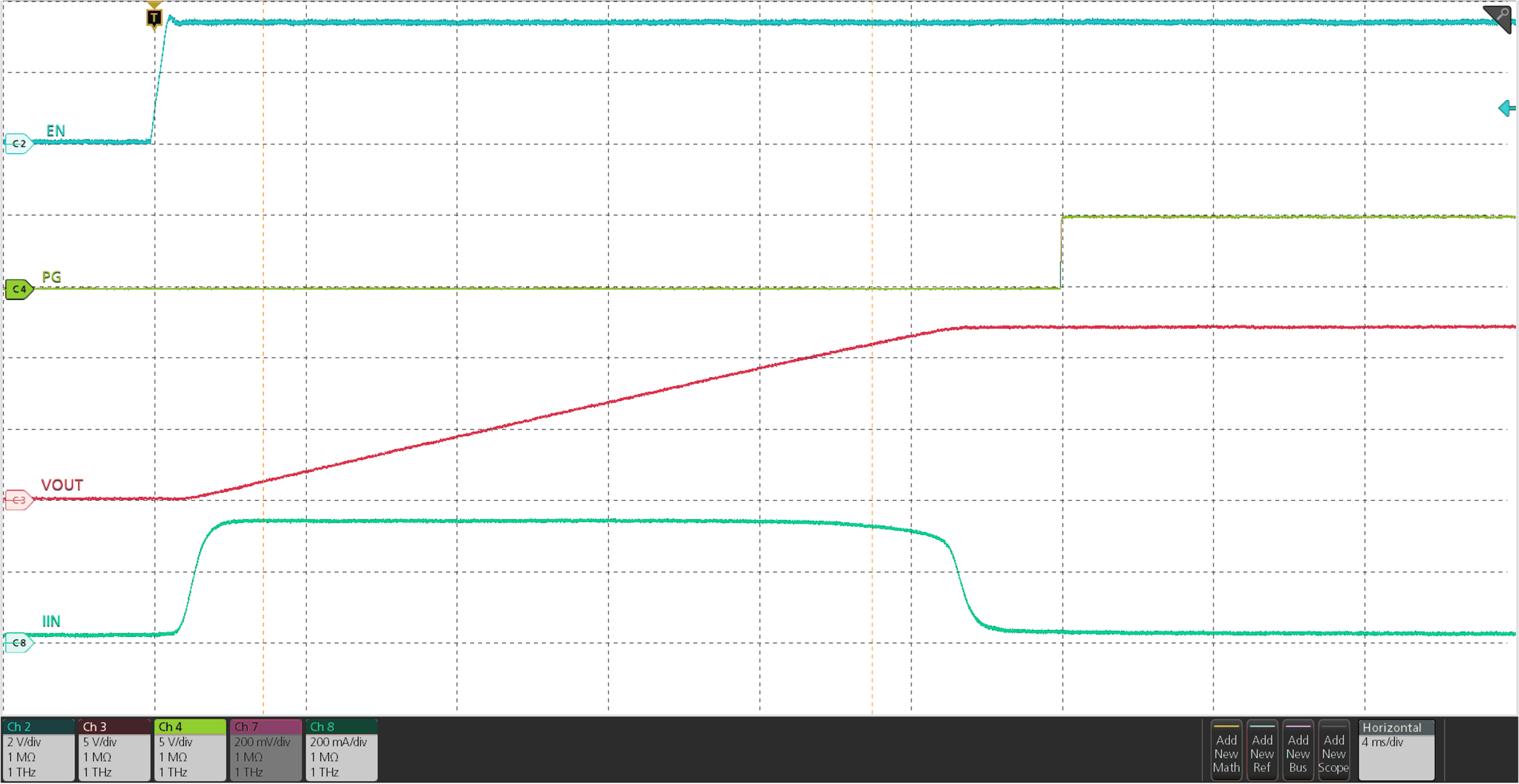
| VIN = 12 V, COUT = 470 μF, CdVdt = 5100 pF, VEN/UVLO stepped up to 3.3 V |
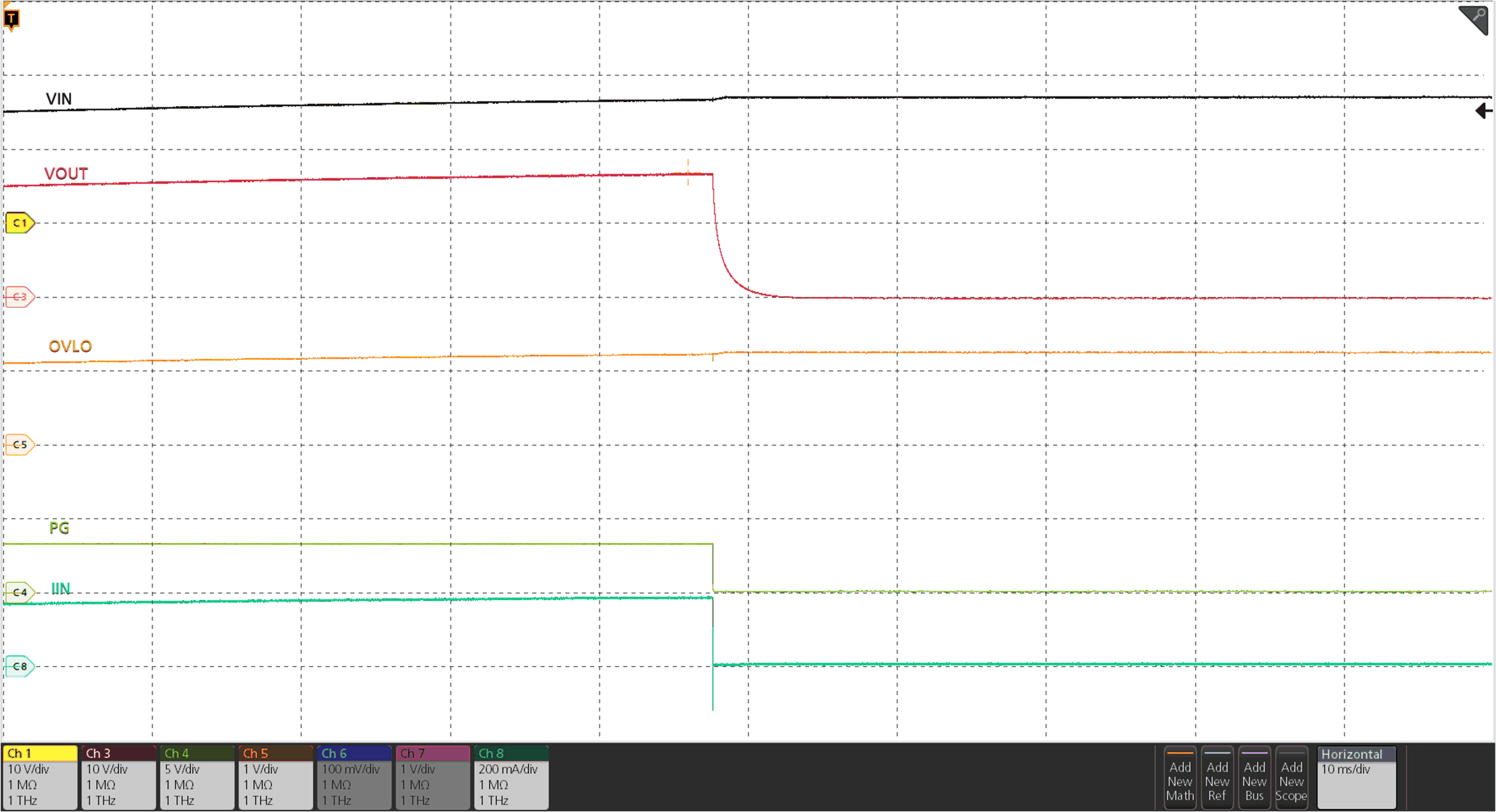
| OV threshold set to 16.7 V, VIN ramped up from 12 V to 17 V |
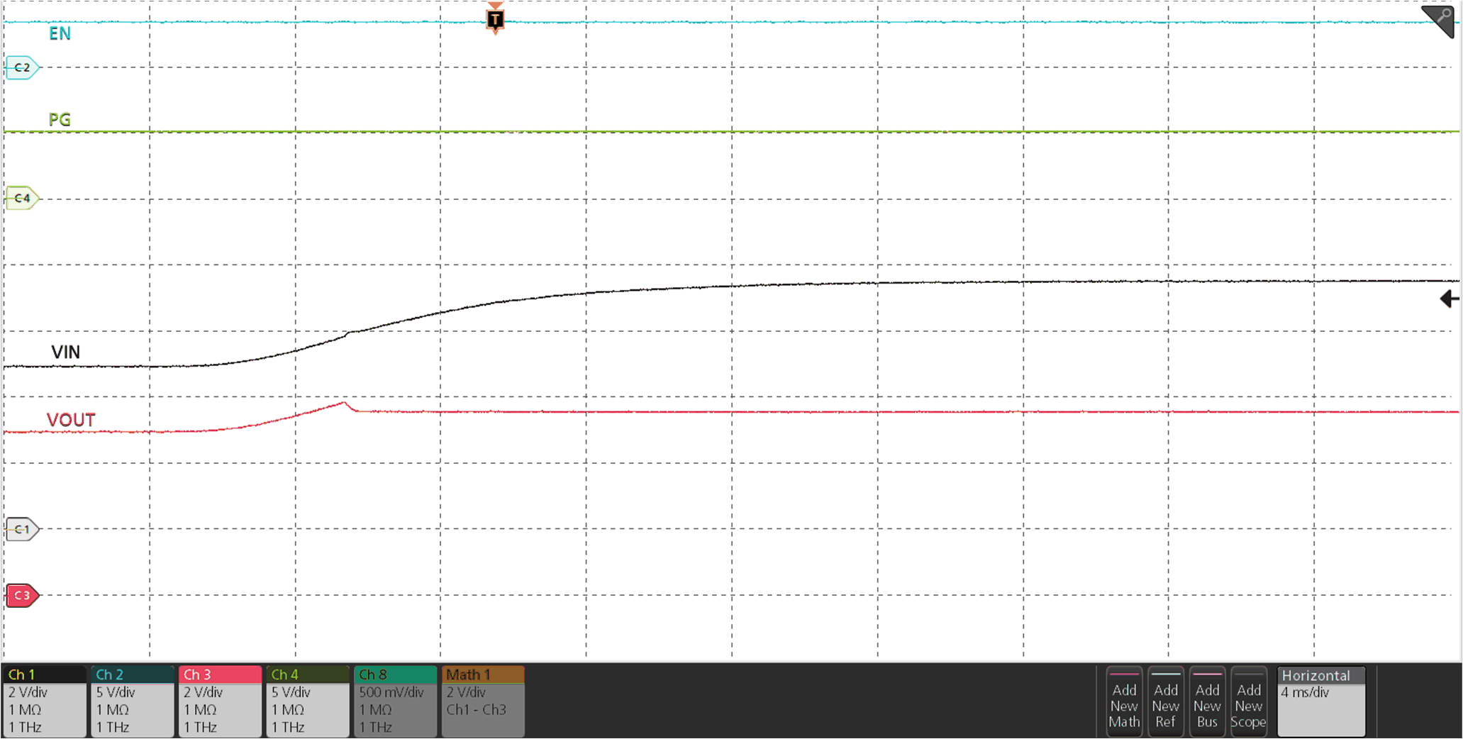
| ROVCSEL = Open, COUT = 220 μF, IOUT = 200 mA, VIN ramped up from 5 V to 7.5 V |
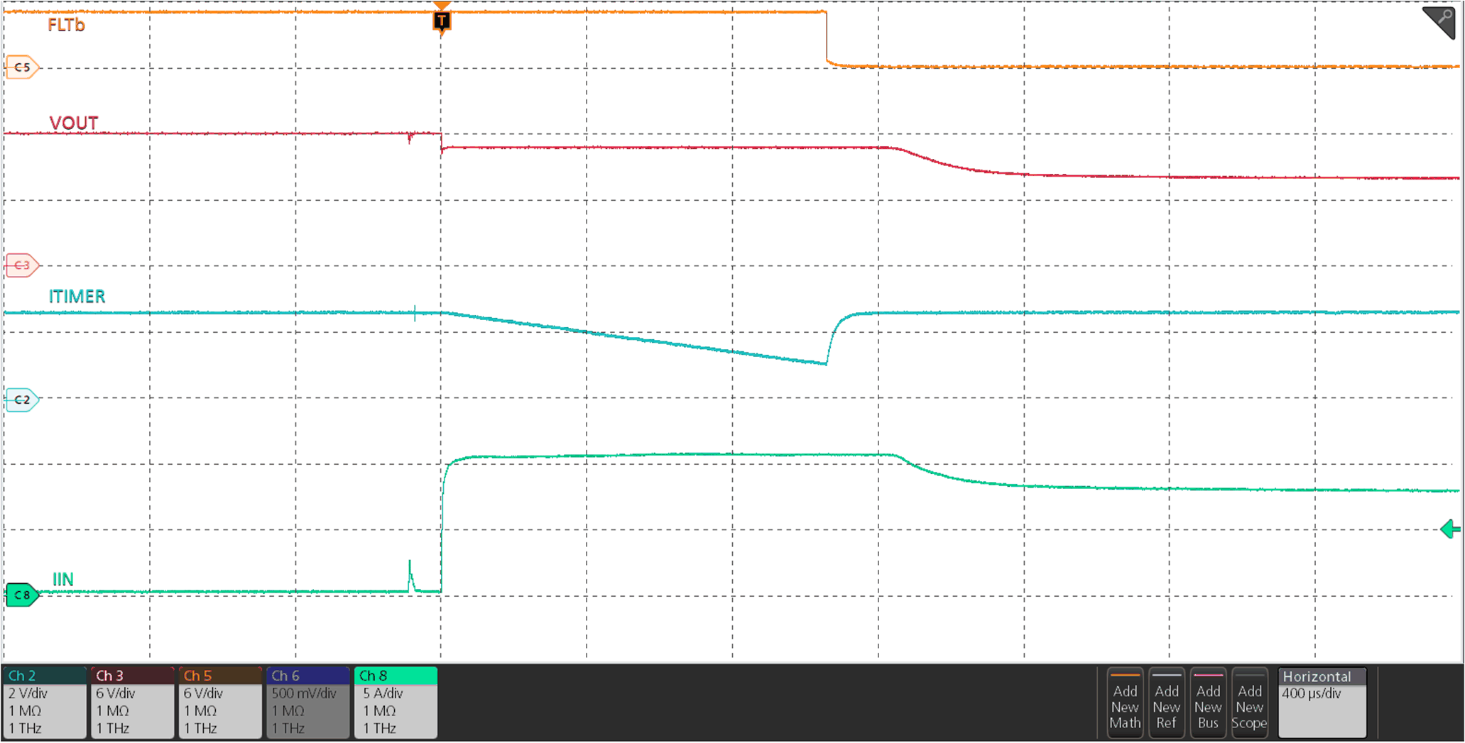
| VIN = 12 V, CITIMER = 1.3 nF, COUT = 220 μF, RILM = 715 Ω, IOUT stepped from 0 A → 11 A |
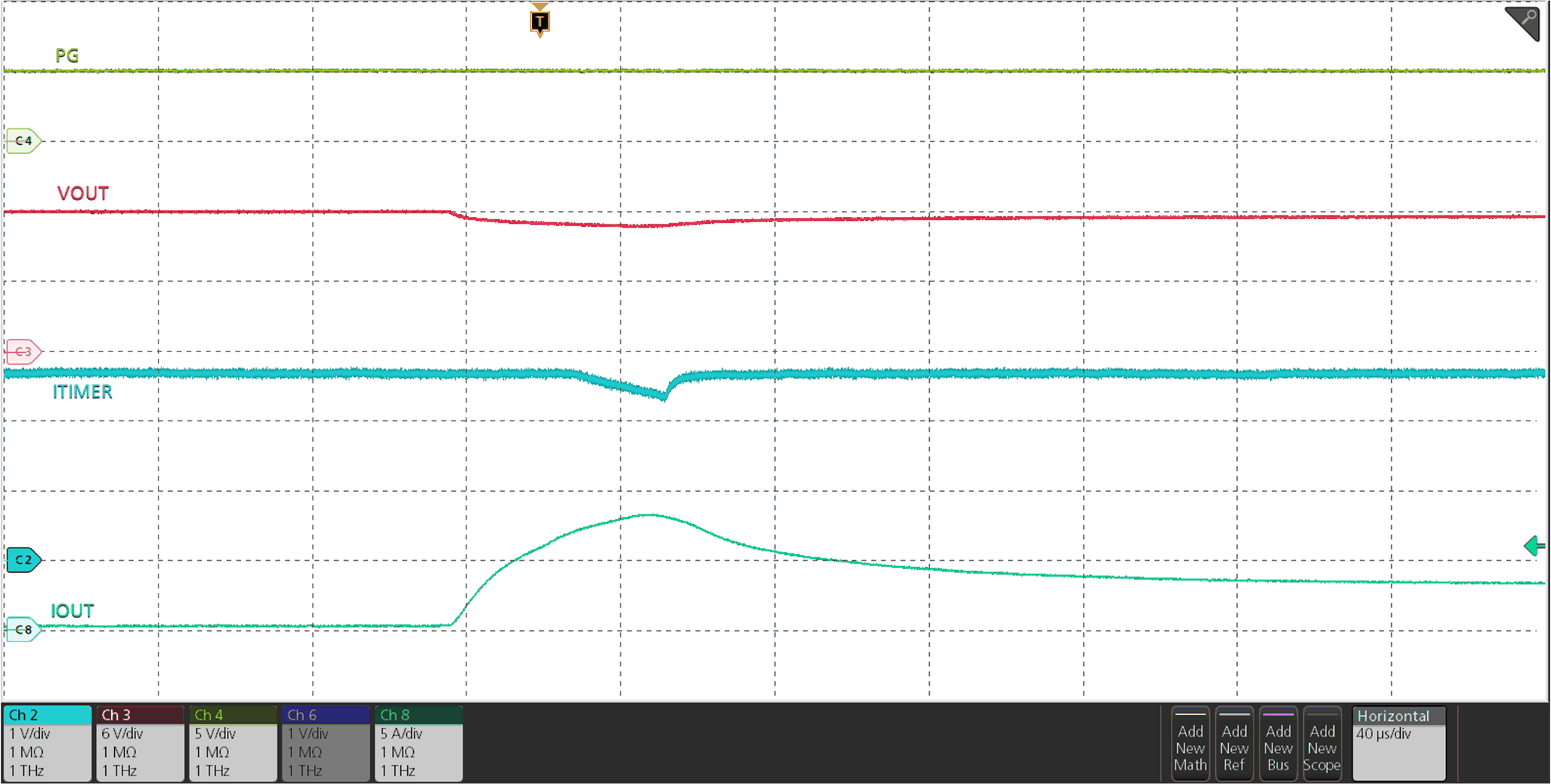
| VIN = 12 V, CITIMER = 120 pF, COUT = 470 μF, RILM = 715 Ω, IOUT ramped from 0 A → 8 A→ 4 A within 100 μs |
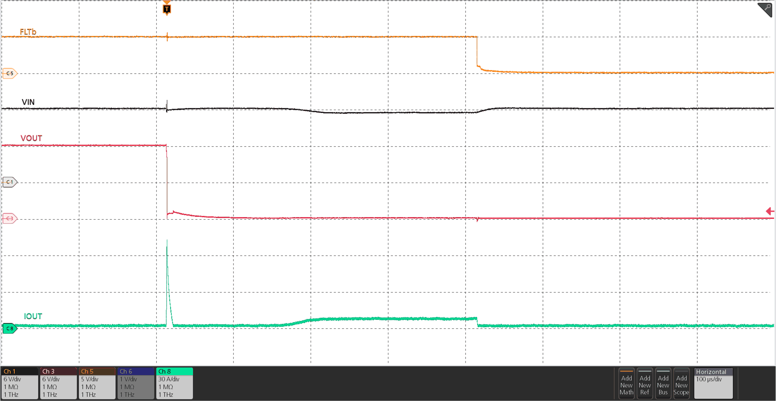
| VIN = 12 V, RILM = 715 Ω, OUT stepped from Open → Short-circuit to GND |
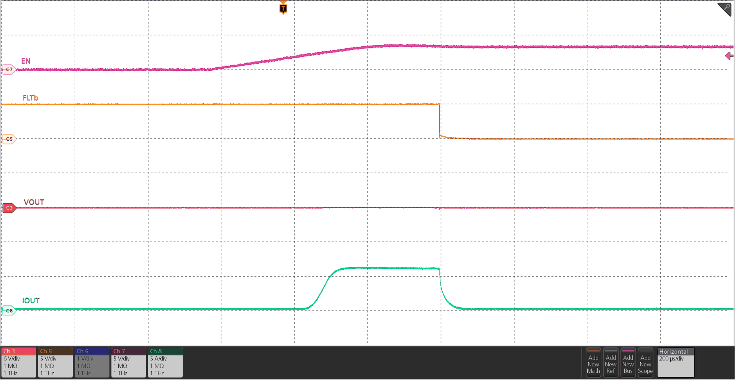
| VIN = 12 V, COUT = Open, OUT short-circuit to GND, RILM = 715 Ω, VEN/UVLO stepped from 0 V to 3.3 V |