ZHCSOF9B april 2022 – june 2023 TPS25981
PRODUCTION DATA
- 1
- 1 特性
- 2 应用
- 3 说明
- 4 Revision History
- 5 Device Comparison Table
- 6 Pin Configuration and Functions
- 7 Specifications
-
8 Detailed Description
- 8.1 Overview
- 8.2 Functional Block Diagram
- 8.3
Feature Description
- 8.3.1 Undervoltage Lockout (UVLO and UVP)
- 8.3.2 Overvoltage Lockout (OVLO)
- 8.3.3 Inrush Current, Overcurrent, and Short-Circuit Protection
- 8.3.4 Analog Load Current Monitor
- 8.3.5 Overtemperature Protection (OTP)
- 8.3.6 Fault Response and Indication (FLT)
- 8.3.7 Power Good Indication (PG)
- 8.3.8 Quick Output Discharge (QOD)
- 8.3.9 Reverse Current Blocking FET Driver
- 8.4 Device Functional Modes
- 9 Application and Implementation
- 10Power Supply Recommendations
- 11Layout
- 12Device and Documentation Support
- 13Mechanical, Packaging, and Orderable Information
9.2 Typical Application
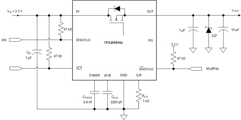
TPS259814x can be used for optical module power rail protection. Optical modules are commonly used in high-bandwidth data communication systems such as optical networking equipment, enterprise/data-center switches and routers. Several variants of optical modules are available in the market, which differ in the form-factor and the data speed support (Gbit/s). Of these, the popular variant double dense quad small form-factor pluggable (QSFP-DD) module supports speeds up to 400 Gbit/s. In addition to the system protection during hot-plug events, the other key requirement for optical module is the tight voltage regulation. The optical module uses 3.3-V supply and requires voltage regulation within ±5% for proper operation.
A typical power tree of such system is shown in Figure 9-7. The optical line card consists of DC-DC converter, protection device (eFuse) and power supply filters. The DC-DC converter steps-down the 12 V to 3.3 V and maintains the 3.3-V rail within ±2 %. The power supply filtering network uses ‘LC’ components to reduce high frequency noise injection into the optical module. The DC resistance of the inductor ‘L’ causes voltage drop of around 1.5% which leaves us with a voltage drop budget of just 1.5% (3.3 V × 1.5% = 50 mV) across the protection device. Considering a maximum load current of 5.5 A per module, the maximum ON-resistance of the protection device must be less than 9 mΩ. TPS259814x eFuse offers a very low ON-resistance of 6 mΩ (typical), thereby meeting the target specification with additional margin to spare and simplifying the overall system design.
 Figure 9-7 Power Tree Block Diagram
of a Typical Optical Line Card
* Optional circuit components needed for transient protection depending on input and output inductance. Please refer to Transient Protection section for details.
Figure 9-8 Optical Module Port Protection