ZHCSTG6A July 2023 – October 2023 TPS25984
PRODUCTION DATA
- 1
- 1 特性
- 2 应用
- 3 说明
- 4 Revision History
- 5 说明(续)
- 6 Pin Configuration and Functions
- 7 Specifications
-
8 Detailed Description
- 8.1 Overview
- 8.2 Functional Block Diagram
- 8.3
Feature Description
- 8.3.1 Undervoltage Protection
- 8.3.2 Insertion Delay
- 8.3.3 Overvoltage Protection
- 8.3.4 Inrush Current, Overcurrent, and Short-Circuit Protection
- 8.3.5 Analog Load Current Monitor (IMON)
- 8.3.6 Mode Selection (MODE)
- 8.3.7 Parallel Device Synchronization (SWEN)
- 8.3.8 Stacking Multiple eFuses for Unlimited Scalability
- 8.3.9 Analog Junction Temperature Monitor (TEMP)
- 8.3.10 Overtemperature Protection
- 8.3.11 Fault Response and Indication (FLT)
- 8.3.12 Power-Good Indication (PG)
- 8.3.13 Output Discharge
- 8.3.14 FET Health Monitoring
- 8.3.15 Single Point Failure Mitigation
- 8.4 Device Functional Modes
- 9 Application and Implementation
- 10Device and Documentation Support
- 11Mechanical, Packaging, and Orderable Information
8.3.1 Undervoltage Protection
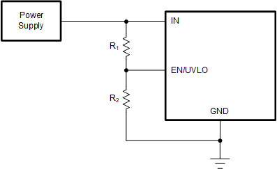
The TPS25984x implements undervoltage lockout on VDD and VIN in case the applied voltage becomes too low for the system or device to properly operate. The undervoltage lockout has a default internal threshold of VUVP on VDD and VUVPIN on VIN. Alternatively, the UVLO comparator on the EN/UVLO pin allows the undervoltage protection threshold to be externally adjusted to a user defined value. Figure 8-1 and Equation 1 show how a resistor divider can be used to set the UVLO set point for a given voltage supply.
 Figure 8-1 Adjustable Undervoltage Protection
The EN/UVLO pin implements a bi-level threshold.
- VEN > VUVLO(R): Device is fully ON.
- VSD(F) < VEN < VUVLO(F): The FET along with most of the controller circuitry is turned OFF, except for some critical bias and digital circuitry. Holding the EN/UVLO pin in this state for > tQOD activates the Output Discharge function.
- VEN < VSD(F): All active circuitry inside the part is turned OFF and it retains no digital state memory. It also resets any latched faults. In this condition, the device quiescent current consumption is minimal.